
1930 ~ 1990MHz narrow-band RF2320 linear amplification circuit diagram
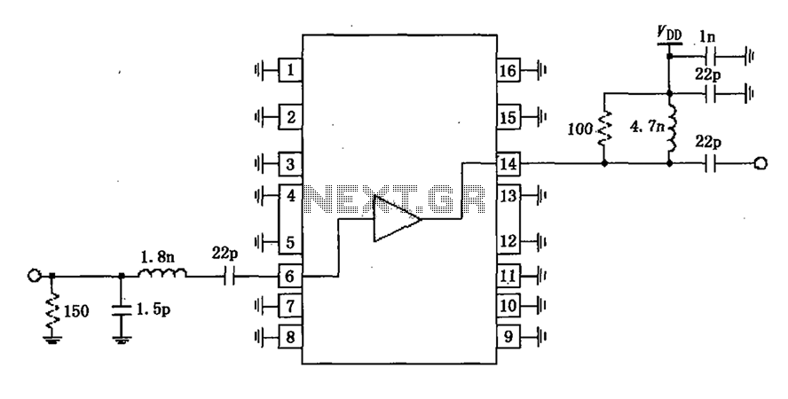
The described narrowband linear amplifier circuit utilizes the RF2320, which is specifically designed for high-frequency applications. The operational frequency range of 1930 to 1990 MHz makes it suitable for various RF communication systems. The input RF signal is received from a distance of 6 feet, where it is amplified through the internal amplifier positioned 14 feet from the input source.
The direct coupling of the internal amplifier to the input signal path is an essential design choice, as it minimizes signal loss and preserves the integrity of the RF signal. However, this configuration requires the integration of a blocking coupling capacitor to prevent DC components from affecting the amplifier's performance. The typical gate voltage at the input terminal is set to 0V, establishing a baseline for signal amplification. Increasing the external gate bias voltage will lead to a rise in the output current; however, it is crucial to note that this adjustment does not enhance the linearity of the amplifier, which is a critical parameter in RF applications to ensure signal fidelity.
The output of the amplifier, located 14 feet away, is designed to provide both the amplified RF signal and the necessary internal bias. The absence of DC blocking capacitors within the RF2320 chip necessitates the use of an external 22pF capacitor. This capacitor serves as a DC blocking element, allowing only the AC components of the amplified signal to pass while preventing any DC offset from affecting downstream components.
To optimize performance, an output matching network is implemented to align the output impedance of the amplifier with the load impedance. This matching network is vital for achieving maximum output power and efficiency, which are critical for effective RF signal transmission. By ensuring that the amplifier is properly matched to its load, signal reflections are minimized, and power transfer is maximized, leading to improved overall system performance.1930 ~ 1990MHz as shown in Fig narrowband linear amplifier circuit configured by RF2320. Radio frequency (RF) signal input from 6 feet, after amplified by an amplifier 14 feet out. 6 feet and internal amplifier is directly coupled, so plus a blocking coupling capacitor. Typically, the gate voltage of the input terminal is 0V, but the external gate bias voltage increases will increase, which will increase while the current, but will not improve amplifier linearity. 14 feet while providing outputs and internal bias, not in the chip DC blocking capacitors, and the pin dc voltage, so a 22pF capacitor as a DC blocking capacitor.
Output matching network to match the output impedance of the amplifier, in order to obtain the maximum output power and efficiency.
Related Circuits
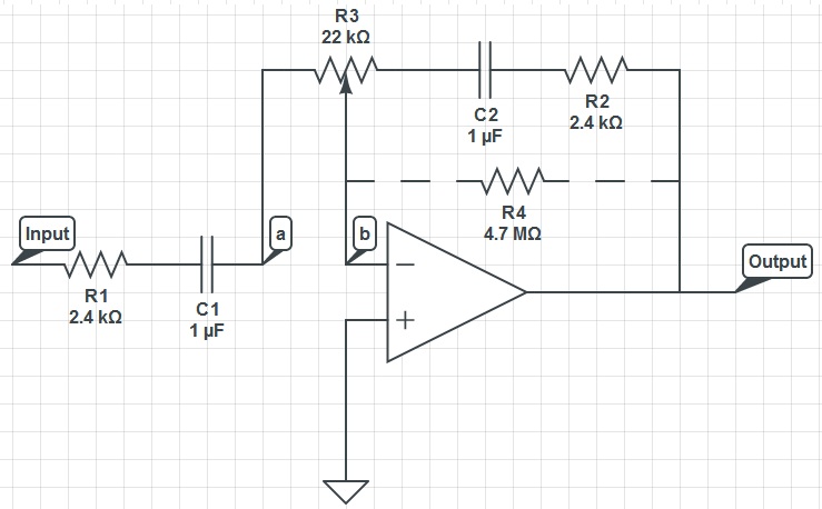
This circuit can function as a treble control circuit, with high-frequency gain occurring when resistor R3 is set to a value that makes points a and b equal (denoted as k=0). Conversely, high-frequency attenuation occurs when R3 is set...
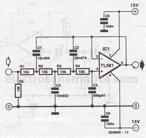
A Butterworth filter is a type of filter characterized by a frequency response that is flat within the passband region. This filter was first described by British engineer Stephen Butterworth. A Butterworth filter is designed to provide a maximally flat...
This is an aerial current power supply with a continuously adjustable stabilized output ranging from 0 to 30VDC. The circuit also incorporates an electronic current limiter that effectively controls the output current from a few milliamperes (2 mA) to...
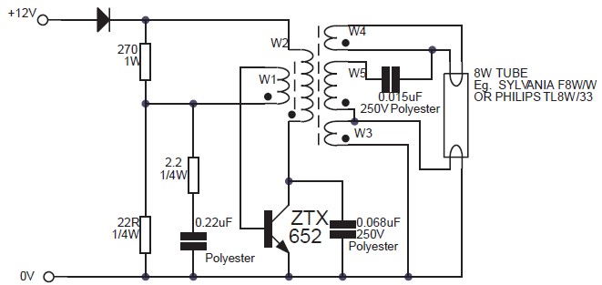
This circuit is an 8W inverter designed to drive an 8W fluorescent lamp from a 12V power supply, utilizing an inexpensive inverter based on a ZTX652 transistor. The inverter operates from power supplies ranging from 10V to 16.5V, achieving...
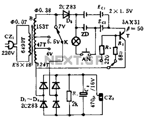
This circuit is designed for high current applications using nickel-cadmium rechargeable batteries, and it can also function as a general low-voltage DC power supply. The circuit consists of a charging section and a DC output section. K2 serves as...
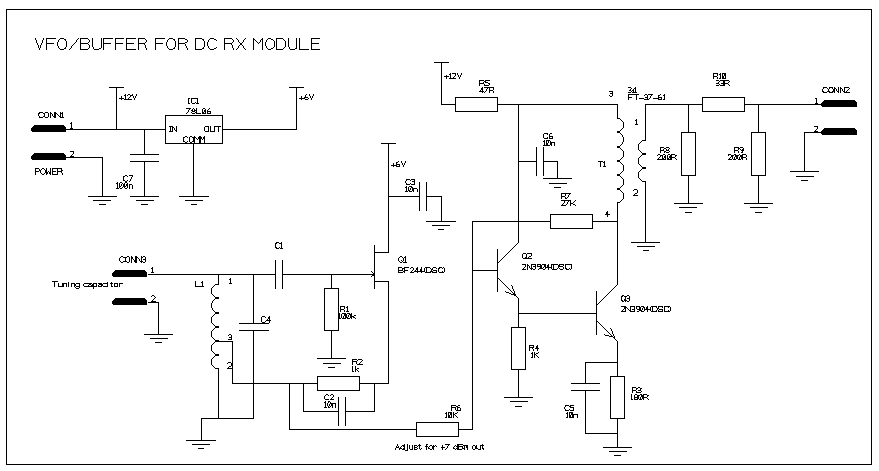
It is essentially a standard Hartley oscillator, with an output of +7 dBm into 50 Ohms. It is advised against adding a gate diode, as this circuit does not require it and such an addition would degrade phase noise...
Warning: include(partials/cookie-banner.php): Failed to open stream: Permission denied in /var/www/html/nextgr/view-circuit.php on line 713
Warning: include(): Failed opening 'partials/cookie-banner.php' for inclusion (include_path='.:/usr/share/php') in /var/www/html/nextgr/view-circuit.php on line 713