
2500W Phase Control with TLE3103

The circuit is designed to control both resistive and inductive loads, making it versatile for various applications. The main component, the Siemens TLE3103, functions as a phase control circuit, enabling precise control of the power delivered to the load. This is achieved through its integrated power supply and zero voltage crossing detector, which ensures that the triac (BTA41) is triggered at the optimal point in the AC waveform, minimizing electrical noise and potential damage to the load.
The logic driver associated with the TLE3103 can be enabled or disabled through a low voltage input, allowing for flexible control of the triac's firing mechanism. When pin 13 of the TLE3103 is left open (floating), the trigger output remains active; however, grounding this pin disables the trigger output, providing a straightforward method to control the power output based on external conditions.
User interaction with the circuit is facilitated through two pushbuttons, which control a 32-step digital potentiometer (AD5228). The potentiometer's position can be adjusted based on user inputs, allowing for fine-tuning of the load's power level. The MAX6817 debouncer IC ensures that the pushbutton signals are clean and free from noise, which is critical for reliable operation.
The digital potentiometer features a power-on reset pin that can be configured via jumper JP1. This allows the potentiometer to start at either midscale or zero scale, depending on whether the pin is connected to ground or VCC, respectively. This feature enhances the usability of the circuit by providing a predictable starting state.
The triac selected for this application, the BTA41, is rated for loads up to 40A, which exceeds the requirements for controlling loads up to 2,500W. Its isolated body design enhances safety when handling the circuit, particularly under voltage conditions.
Additionally, the snubber circuit, which is crucial for protecting the triac from voltage spikes, is designed with a 68µH inductance. It can be replaced with a 100Ω resistor if necessary, although care should be taken to adjust capacitor C5 to 47nF in this case to maintain circuit stability and performance.
The circuit board is single-sided, measuring 3.54 x 2.15 inches (87.63 x 54.61 mm), which simplifies manufacturing and assembly processes. The MAX6817 debouncer, housed in a SOT23-6 package, can be soldered directly onto the board or adapted for use with a DIP-6 package, providing flexibility in design and assembly.
Overall, this circuit represents a robust solution for controlling high-power resistive and inductive loads, with features that enhance both functionality and safety.This circuit controls resistive and inductive loads up to 2,500W. Its main functional device is an integrated phase control circuit - Siemens TLE3103. It contains its own power supply, a zero voltage crossing detector circuit and a logic driver. An additional feature is the low voltage input to enable/disable triac firing enabling/disabling the logic driver. The function is as follows: pin13 TLE3103 open (floating), trigger output active, tied to ground trigger output disabled.
An UP and a DOWN pushbutton control a 32-step digital potentiometer (IC2, AD5228) via the debouncer IC1 (MAX6817). The digital potentiometer has a power on reset pin which might be tied to ground causing the potentiometer to start at midscale, or to VCC causing it to start at zero scale.
The desired function is selectable using jumper JP1. The triac (capable of driving 40A loads) is a bit overkill for the desired power but the BTA41 has an isolated body and therefore handling of the board under voltage is less dangerous as it is with phase on the package. The snubber circuit uses a 68?H inductance but this might be replaced with a 100 resistor. When replacing the inductance C5 should have a value of 47nF. Board: Purely single sided, measurements: 3.54X2.15 inches (87.63X54.61mm) Remark: The debouncer circuit is manufactured with a SOT23-6 package.
It might be soldered directly onto the board (DIP-6 package) using thin wires or an adapter board. Part Value Package C1 100n C-5 C2 100n C-5 C3 100/16 ELC3,81 C4 22n C-5 C5 10n/250VAC C-15 D1 1N4005 DO41-10 IC1 MAX6817 AD-SOT23 IC2 AD5228 DIL08 IC3 TLE3103 DIL-14 J1 TE-03 TERMINAL 5.08 J2 TE-03 TERMINAL 5.08 J3 TE-03 TERMINAL 5.08 L1 68H/3A DS30A Q1 BTA41-600 TOP3 R1 120R R-10 R2 18K/2W R-18 R3 820K R-10 R4 180K R-10 R5 56K R-10 S1 UP BUTTON-02 S2 DOWN BUTTON-02 🔗 External reference
Related Circuits
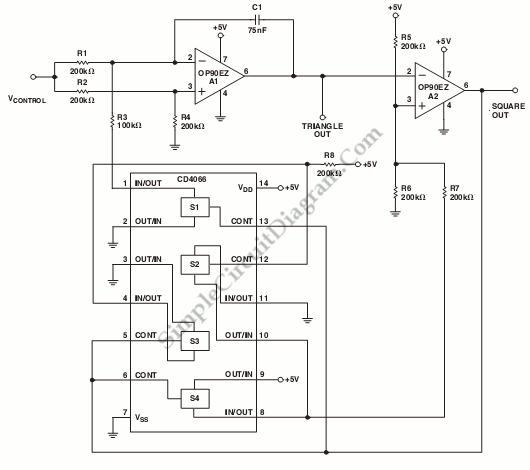
This is a schematic diagram of a micropower voltage-controlled oscillator circuit. This circuit can generate square and triangle wave outputs and only requires minimal power. The micropower voltage-controlled oscillator (VCO) circuit is designed to produce both square and triangle waveforms,...
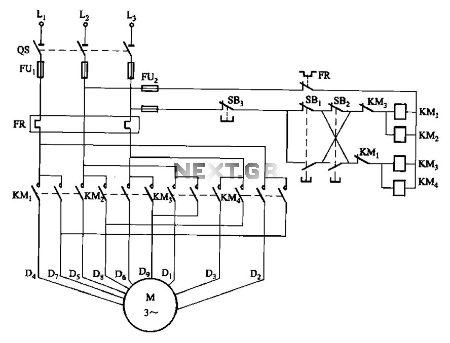
The circuit depicted in Figure 3-112 features two operation buttons: SBi, which serves as the first speed operation button, and SBz, which operates the second speed class. Both buttons facilitate two speeds in the same direction. The circuit design incorporates...
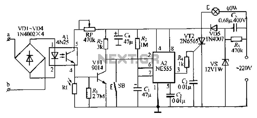
The lamp base circuit integrates an NE555 timer and optocouplers to automatically activate the light when a phone call is received at night. The lamp will self-extinguish after a delay. Additionally, a switch allows manual control of the lamp....
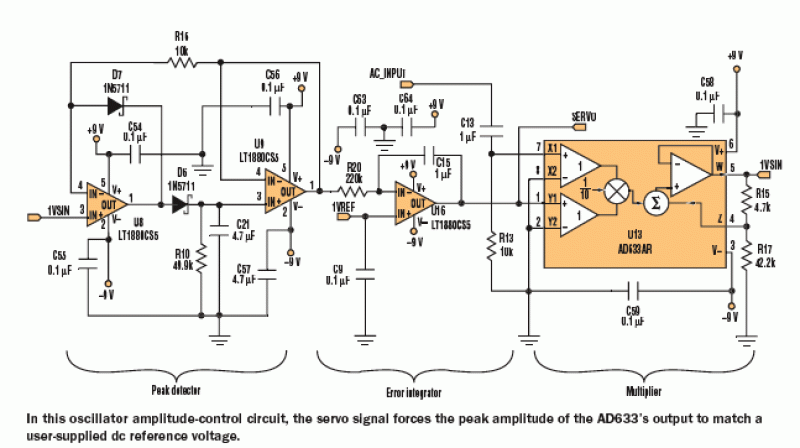
The figure illustrates a schematic for an oscillator amplitude-control servo system. The circuit establishes a closed-loop system that provides a fixed and adjustable peak-to-peak amplitude AC signal centered around 0 V. A 1 kHz sine wave, designated as AC_INPUT,...
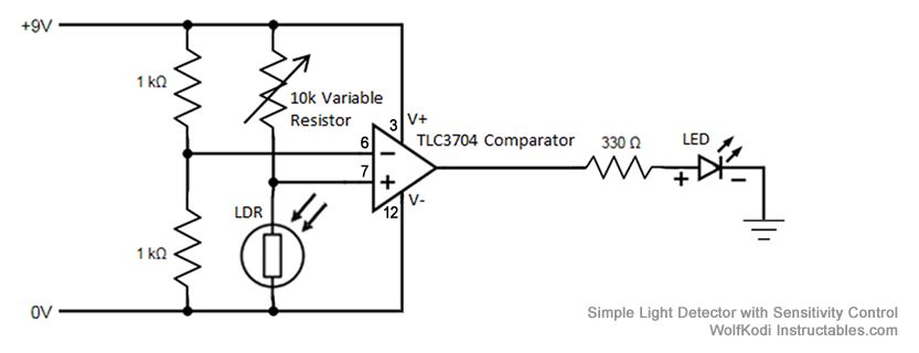
The schematic diagram for the circuit is provided in the accompanying image. As indicated by its name, a comparator is designed to compare two specified voltages. The circuit includes a pair of 1K resistors. A comparator circuit typically utilizes operational...
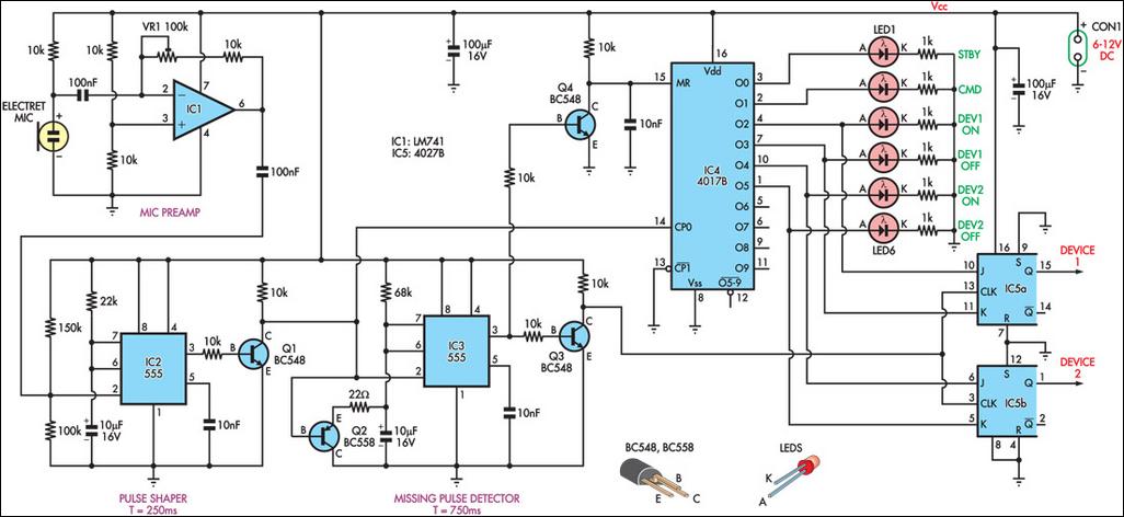
This circuit can switch two or more devices on and off in response to a series of rapid handclaps. The claps are detected by an electret microphone and amplified by a 741 operational amplifier (IC1). IC1 is configured as...