
5V TOP414G 2A isolated switching power supply circuit
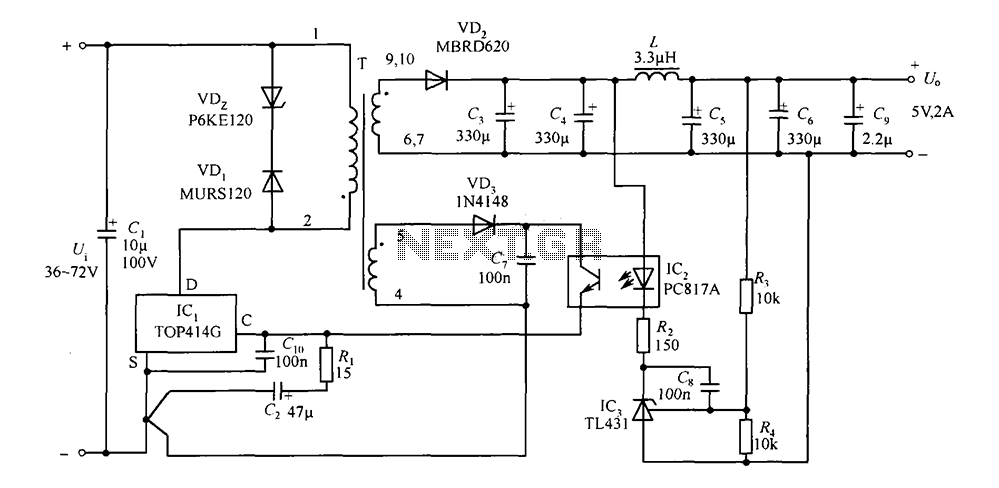
The described circuit is a robust solution for generating a stable 5V output from an isolated switching power supply. The use of the TOP414G provides efficient power conversion with a maximum output current of 2A, making it suitable for various applications requiring stable voltage regulation. The input filter capacitor, C1, is essential for reducing voltage spikes and noise from the power supply, ensuring that the circuit operates reliably.
The voltage clamp protection provided by VD1 is critical for safeguarding the circuit against over-voltage conditions, which could potentially damage sensitive components. The combination of R1 and C2 at the control terminal serves to stabilize the control loop and improve transient response by filtering out high-frequency noise.
The parallel connection of TOP414GC-S with C10 is a strategic design choice aimed at enhancing the overall stability of the switching power supply. It helps prevent high-frequency interference from affecting the operation of the control circuit, thereby reducing the likelihood of unwanted power outages.
The output stage of the circuit, which includes VD2, C3, C4, L, C5, and C6, is designed to ensure that the output voltage remains within specified limits while minimizing ripple and noise. C9 plays a vital role in noise cancellation, further enhancing the quality of the output voltage.
The TL431 shunt regulator is an effective choice for providing feedback control in this application. It allows for precise regulation of the output voltage by comparing the sampled voltage from R3 and R4 against its internal reference voltage. The resulting control signal adjusts the duty cycle of the TOP414G, maintaining a stable output voltage despite variations in load or input voltage.
The feedback winding voltage, rectified by VD3 and C7, powers the infrared receiver of the PC817A, ensuring that the optocoupler operates effectively. This isolation between the control and output stages is crucial for protecting sensitive components from potential faults in the output circuit.
Overall, this circuit design demonstrates a well-thought-out approach to creating a reliable and efficient isolated switching power supply, suitable for a variety of electronic applications requiring 5V power.Constituted by a 5V TOP414G, 2A output isolated switching power supply circuit is shown. C1 is the input filter capacitor. VDz VD1 composition and primary clamp protection circ uit. The control terminal of the resistor R1, C2 is a bypass capacitor. TOP414GC-S parallel between the end of the C10 is to prevent high-frequency interference appears on the control side sometimes cause power outages trigger circuit malfunction. VD2 output rectifier diode, output filter C3, C4, L, C5 and C6 constituted, C9 as an output capacitor noise cancellation.
External error amplifier by a TL431 shunt regulator composition. When the output voltage fluctuates, by R3, R4 after the voltage obtained by dividing the sample voltage, the TL431 with a reference voltage, and generates an external control signal, and then to change TOP414G control terminal current through optocoupler PC817A, thereby regulating the duty than make Uo stabilize. Control loop gain is set by R2. After the feedback winding voltage VD3, after C7 rectifier to PC817A the infrared receiver power supply.
Related Circuits
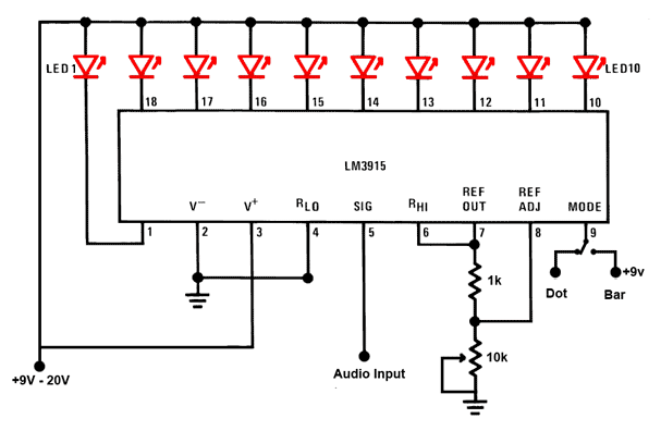
This is a simple audio sound level LED display circuit diagram. The circuit is entirely based on a single integrated circuit, the LM3915 from National Semiconductor. The LM3915 is a monolithic integrated circuit that displays the audio sound level...
This is a solar tracking circuit designed to harness power from sunlight. The circuit operates optimally by maximizing sunlight exposure to generate electricity. The solar tracking circuit utilizes a combination of photovoltaic (PV) cells, sensors, and a microcontroller to adjust...
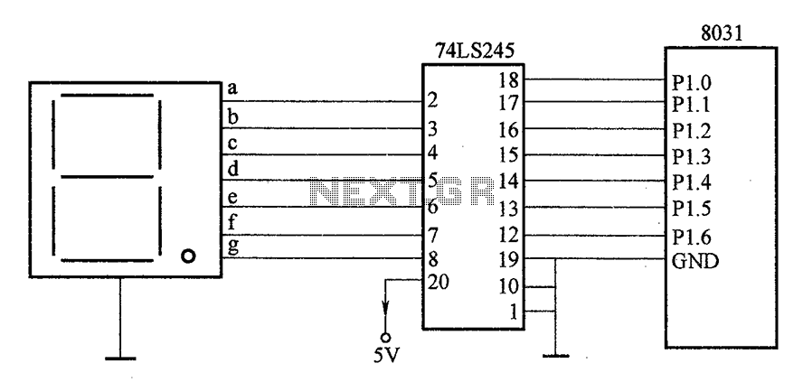
After the SCM execution, the Pl output port connects to the bidirectional input of 74LS245 driver chips. This driver operates during each phase of digital control, based on the information from the Pl port. The purpose is to convert...
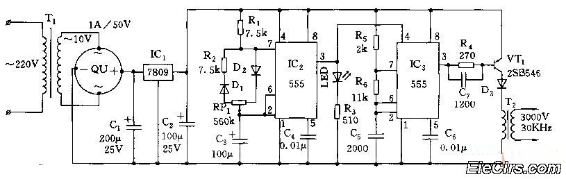
Adjust the RP1 to modify the pulse duty cycle of IC2, which in turn alters the pulse oscillation time of IC3. This regulation allows for the control of ozone generation time, effectively changing the concentration of ozone in the...
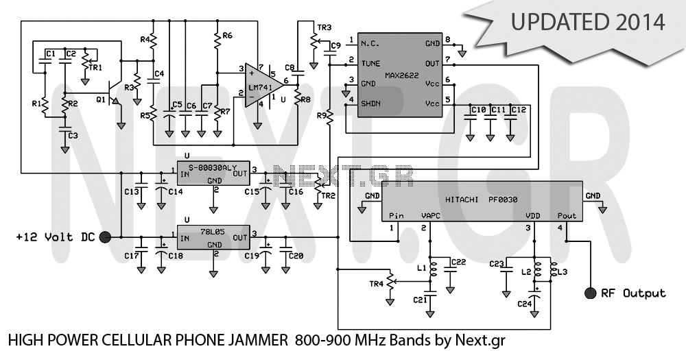
UPDATED 2014 This project presents the original high-power mobile phone jammer circuit, with all updates posted here. Caution is advised regarding the use of this device, as it is illegal. The purpose of sharing this circuit is solely for...
Telephones are declining globally; however, India has over 350 million mobile phone users, alongside a significant number of traditional telephone users. This telephone timer is designed to save costs by controlling unnecessary time spent during phone calls. This simple...