
A functional block diagram of the MC1428
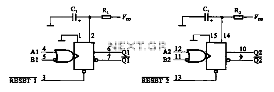
The MC14528 is a versatile integrated circuit designed for monostable applications, where it produces a single pulse output in response to a triggering signal. The block diagram typically includes several key components: the trigger input, timing capacitor, resistor, and output stage.
The trigger input allows external signals to initiate the monostable operation. Upon receiving a trigger pulse, the internal circuitry activates the timing mechanism, which is primarily determined by the external resistor and capacitor values connected to the IC. The duration of the output pulse is defined by the RC time constant, which can be adjusted to meet specific timing requirements.
The output stage of the MC14528 is capable of driving various loads, making it suitable for a wide range of applications, including timing circuits, pulse generation, and signal conditioning. The dual monostable trigger design enhances its functionality, allowing users to implement multiple timing events within a single circuit, thereby simplifying design complexity and saving space on the printed circuit board.
Overall, the MC14528 monoflop is an essential component for engineers seeking reliable timing solutions in digital circuits, offering flexibility and ease of use in various electronic applications.A functional block diagram of the MC1428 Monoflop shown a functional block diagram of an integrated circuit MC14528. The IC features two monostable trigger road, more convenien t to use.
Related Circuits

A differential amplifier with input impedance as indicated in the circuit diagram. A differential amplifier is a crucial component in various electronic applications, primarily used to amplify the difference between two input voltages while rejecting any common-mode signals. This characteristic...
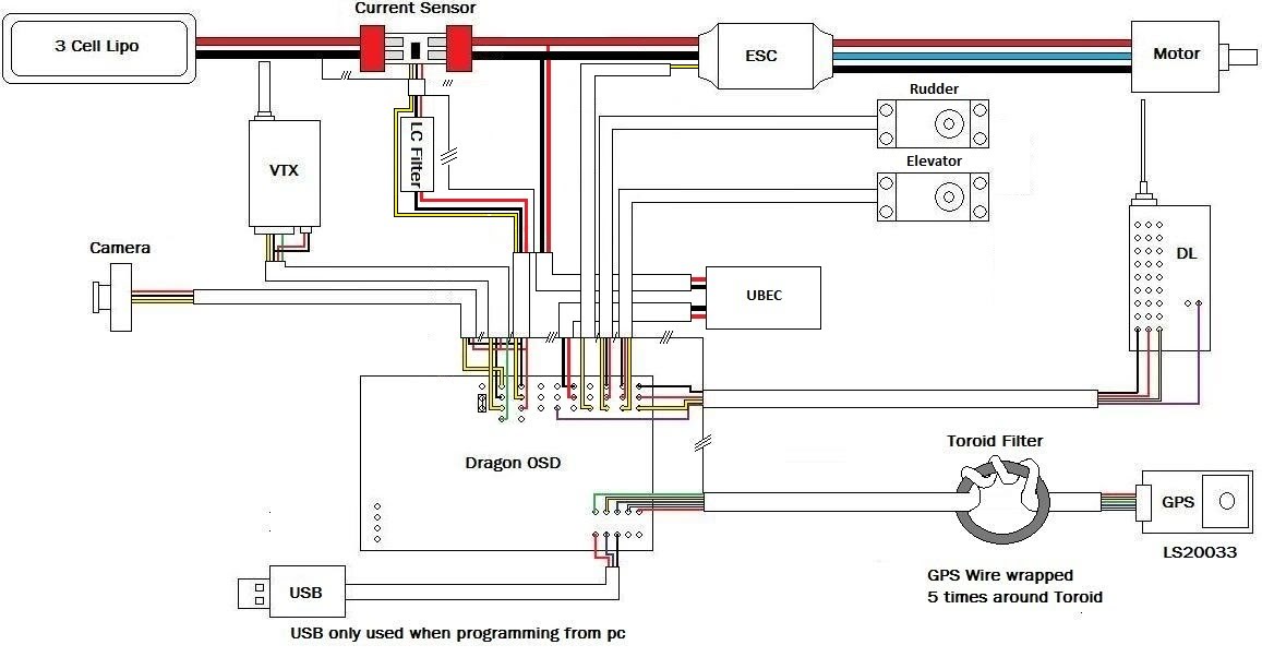
A discussion has been initiated regarding the diagrams being created. The initial set pertains to the DOSD (Dual OSD). Following the discovery of a potential issue, these new diagrams will facilitate safe wiring of the DOSD, thereby avoiding the...
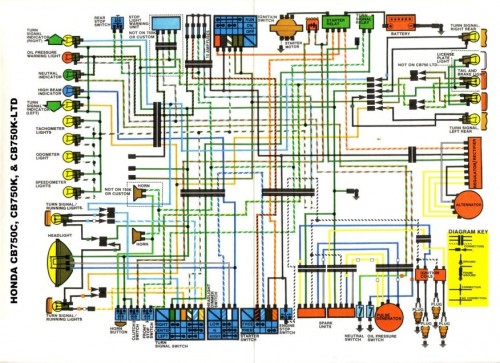
Many inquiries arise regarding motorcycle wiring, particularly among individuals attempting to repair their blinkers or seeking to streamline electronics for custom builds. A crucial aspect of constructing any chopper, bobber, cafe racer, brat bike, or rat rod involves eliminating...
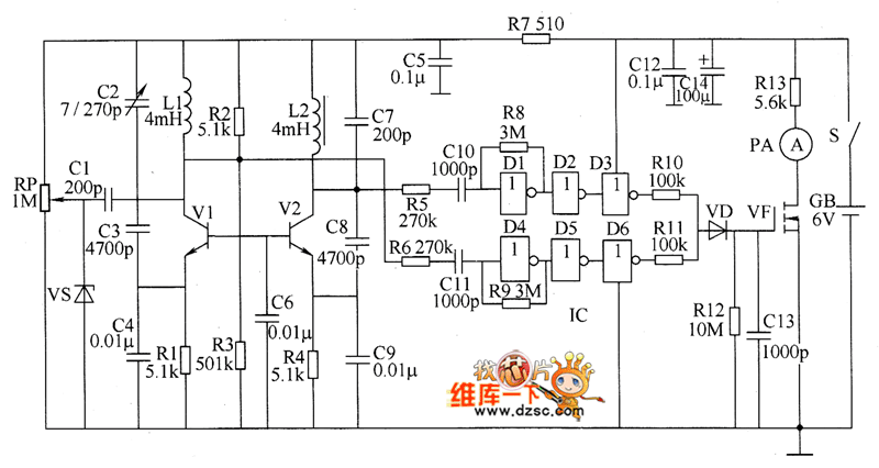
The metal detector circuit consists of several key components including the probe oscillator, reference oscillator, oscillation signal processor, mixing amplifier, and ammeter PA. The probe oscillator is made up of the oscillating tube VI, exploration coil L1, capacitors C1...

A 2004 Chevrolet Impala is experiencing issues with the rear defogger. The owner is unable to locate the fuse for the rear defogger, although the relay has been found. Both the manual and the vehicle's diagram indicate a 30-amp...
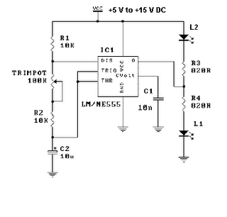
This is a simple LED flasher project that utilizes a common 555 timer integrated circuit (IC) for its operation. It is configured in astable mode, which means its output functions as a square wave oscillator. Two LEDs are connected...