
alternating square pulse generator

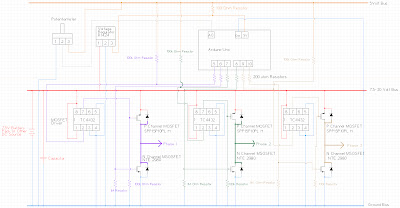
The 4027 dual JK flip-flop is designed to facilitate various digital applications, particularly in systems requiring precise timing and control. Each flip-flop can operate independently, allowing for versatile configurations in toggle and register functions. The logic edge clocking ensures that changes in output states occur synchronously with clock pulses, enhancing reliability in digital circuits. The ability to drive low-power TTL loads makes the 4027 suitable for battery-operated devices, minimizing power consumption while maintaining performance.
The 4001 quad 2-input NOR gate provides essential logic functions, allowing for the construction of complex digital circuits with minimal power requirements. Its high input impedance ensures that it does not load down preceding stages, making it ideal for cascading multiple gates. The capability of each output to drive numerous inputs expands the versatility of the circuit, enabling the design of intricate logic networks.
The pulse generation and counting mechanism described utilizes a combination of flip-flops and counters to create a reliable pulse-width modulation system. The use of a T-flip-flop for frequency division allows for straightforward manipulation of pulse frequencies, while the decimal counter provides a clean and efficient method for counting and controlling sequential operations. The integration of the output stages ensures that the system can handle varying signal levels, allowing for robust performance across different operational conditions.
The conversion of waveforms from sine or triangular shapes to square pulses is critical in many digital applications, and the use of logic gates for this purpose exemplifies the flexibility of the circuit design. The ability to switch between different waveforms using a simple DIP switch enhances user control and adaptability.
Overall, the described circuit leverages the strengths of the 4027 and 4001 components to create a versatile, low-power, and reliable digital system capable of performing a range of functions in various electronic applications.4027 a dual JK flip flop that has independent clock, set, and reset inputs for each flip flop used in toggle, register, and control functions due to its features such as capability of driving two low power TTL loads, logic edge clocked flip flop design, logic swing independent of fanout, toggle rate of 3 MHz at 5 Vdc, supply voltage range of 3 V to 6 V, protection of diodes on all inputs, noise immunity, and quiescent current of 2 nA at 5 Vdc. 4001 a quad 2-input NOR gate integrated circuit, generally characterized by small fluctuation in voltage supply, very high impedance, outputs that can sink and source, one output can drive up to 50 inputs, high speed gate propagation time, high frequency, and low power consumption.
The generator functions without distortion when it reaches 100 KHz. The square pulses are produced when the selector switch S1 is turned ON, which matches the output of Q3 at pin 7. The 5V pulse line is applied to J1 input, the signal is fed to T-flip flop IC1A through S2 which creates pulses indicated at half of the duration time where pin 2 handles the division of pulse frequency.
The pulses are applied to IC2 pin 14 and IC3A input. IC2 acts as decimal counter with decode outputs where each entry produces HIGH on one of the outputs. From the initial pulse entry, the output of Q1 becomes HIGH while others are LOW. The second pulse entry causes HIGH output on Q2, and third entry applies on Q3. The same operation occurs for the succeeding pulse line entry, since the counter checks the number of pulses that passes the generator output.
The generator output stage is considered on levels where the driving stage of Q2 creates positive output voltage and the saturation of Q 3 in the cutoff region. Through the potentiometer, the signal is applied in the output of J2. Using the gates of IC3B-C-D, the sine wave or triangular wave can be changed to square pulses in the circuit input.
The conversion is directly made from the command of S2. The switching can also be done by DIP switch S2. A suitable power supply or two NiCd batteries can maintain the circuit with the stabilization of voltage achieved by two Zener diodes. 🔗 External reference
Related Circuits

The circuit illustrated in Figure 1 generates a precise variable-frequency sine wave intended for use as a general-purpose reference signal. It incorporates an 8th-order elliptic switched-capacitor low-pass filter (IC3), which is clocked by a 100 kHz square wave produced...
One of the primary objectives was to convert a generator into a motor using an Arduino. The process of transforming a simple generator into a motor proved to be particularly challenging with a three-phase generator, necessitating the creation of...
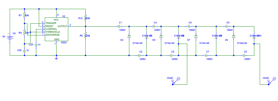
This circuit operates as a 9V DC power source supplying a 555 timer to generate a square wave. The output is then processed through a Half-Wave Series Multiplier (Villard Cascade) to achieve a high voltage DC output. The goal...
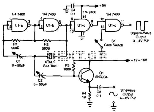
A TTL oscillator utilizing a Quad NAND Gate can operate with fundamental crystals ranging from 1 to 10 MHz. The sine wave output is derived directly from the crystal, which functions as its own filter, producing a relatively clean...
Most metal detectors operate on the principle that metals within a magnetic field alter the behavior of that field. There are two primary methods for detecting these changes. In one method, an alternating current is supplied to a transmit...
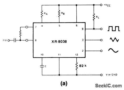
These circuits are similar to that of Fig. 5-47, except that they provide for FM or sweep modulation. Circuit 5-50A is used for FM with small deviations, approximately ±10%. Circuit 5-50B is designed for a sweep range of 1000:1....