
automatic water level circuit
The described circuit employs a 555 timer in a comparator configuration to control a pump or relay based on water level detection. The functionality hinges on the interaction between the Trigger and Threshold pins, which are monitored for voltage levels corresponding to the desired water levels. The use of resistors R1 and R2 ensures that the pins are biased to the supply voltage, allowing for a responsive control mechanism.
In practical applications, the circuit can be utilized in various automated water management systems, such as aquariums, water tanks, or irrigation systems. The design ensures that the pump operates only when necessary, preventing overflow and ensuring efficient water usage. The choice of a 555 timer for this application is advantageous due to its reliability, ease of use, and availability. Additionally, the configuration allows for easy adjustments to the threshold levels by modifying the resistor values, enabling customization based on specific requirements.
Overall, this circuit exemplifies a robust solution for water level detection and control, demonstrating the effective use of operational amplifiers within the 555 timer architecture to achieve desired operational outcomes.Here we are using the Trigger and Threshold pins (2 & 6) to detect the maximum and minimum levels, respectively. The two voltage comparator op-amps inside the 555 control the output, turning it on/off. Looking at the circuit diagram you will notice that the Trigger` pin (2) is marked HIGH probe`, despite being triggered (output goes HIGH) when t
he voltage drops below 1/3 of the supply voltage and, the Threshold` pin (6) is marked LOW probe` while it is reset` (output goes LOW) when the voltage rises above 2/3 of the supply voltage. If this appears to you as being upside-down. One is the GROUND` probe, going to the level a little lower than the minimum desired level. This is the common` (or reference`) probe. The LOW and HIGH probes are set at the desired levels. Resistors R2 and R1 (1M) tie the Trigger` and Threshold` pins (2 & 6) to the positive (+) rail (supply).
In other words, both pins are HIGH. Remember (from above), to make the output of IC1 go HIGH, the trigger pin (2) needs to drop below 1/3 of the supply voltage. (4V with a 12V supply) Since the trigger pin is still HIGH, the output remains LOW. Its purpose is phase reversal. It means that when IC1`s output is HIGH, TR1 conducts and pulls its collector/TR2`s GATE junction LOW, so TR2 is OFF.
Since the pump (or relay coil) is connected between the positive rail (+12V) and TR2`s DRAIN, the pump/relay coil is NOT energized. Now, back to the condition when the IC1`s output is low, TR2`s GATE is HIGH (+12V) and conducting. The pump is operating and water is being filled. As the water level rises, a water bridge` is formed between the GROUND (common) probe and the LOW probe` (Threshold, pin 6) This bridge` constitutes a low resistance, relative to the high resistance of R2 (1M), bringing the voltage at this pin to a low level (at least below 1/3 supply but actual voltage depend on the conductivity of the water).
However, this is IGNORED by IC1 since its output is already LOW (in the reset` mode) When the water level reaches the HIGH probe`, a water bridge` is formed between it and the GROUND probe. Just as with the LOW probe, this bridge` constitutes a low resistance, relative to the high value of R1 (1M), bringing the trigger voltage to below the required level (1/3 supply voltage) and IC1 triggers, its output going HIGH.
Now Tr1 is turned on, the bias voltage/current of TR2 is removed and the pump STOPS. The filling cycle is completed. 🔗 External reference
Related Circuits
VLQC is a quenching circuit developed in the laboratory to meet the specific requirements of an array, including high compactness, cross-talk avoidance, and low afterpulsing. In the VLQC design, a single transistor is utilized to perform the sensing, quenching,...
The high-temperature alarm will emit a beep and the LED will blink when the temperature of the device rises abnormally. This simple overheating alarm is designed to monitor heat levels. The high-temperature alarm circuit is an essential safety device used...
A transistor is an electronic component that allows a small current to control a significantly larger current. This characteristic is valuable in various renewable energy projects and other applications. A basic circuit diagram is provided, featuring a 12V LED...
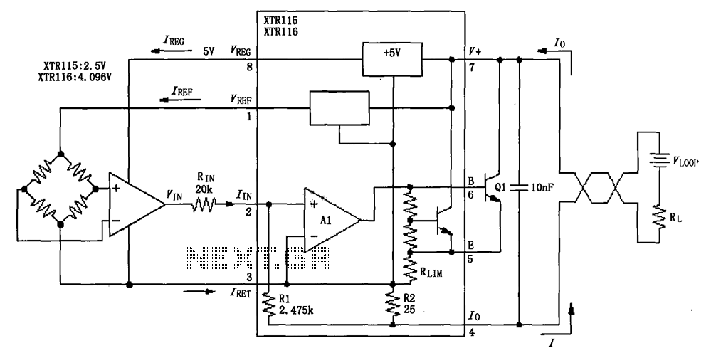
The output reference voltage VREF from the O pin is not utilized within the internal circuit; instead, it is provided to the external circuit. Similarly, the output voltage VREG is also supplied to the external circuit. All current return...
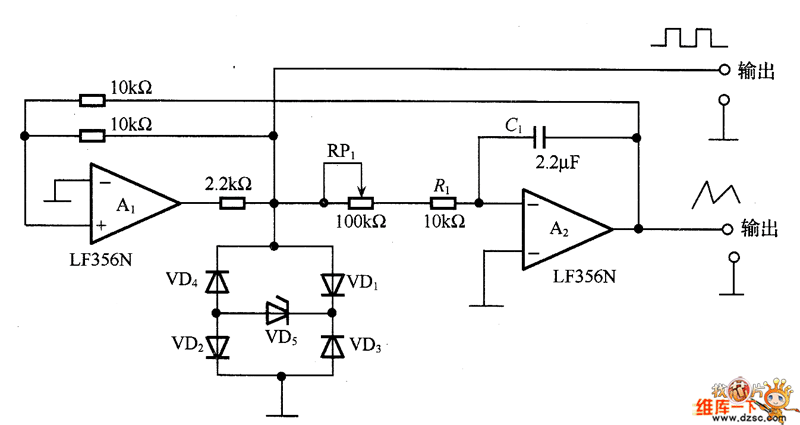
The circuit consists of a lag comparator with amplifier A1 and an inverting integrator A2. The charging and discharging time constant is determined by the integral resistors (R1 + RP1) and the capacitor C1. Diodes VD1 to VD5 form...
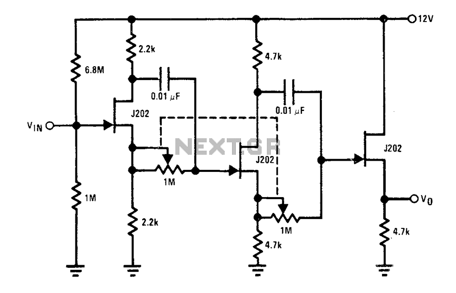
Each J202 JFET stage provides up to 180 degrees of phase shift controlled by a 1 megohm potentiometer. The potentiometer allows for complete control of the groups. JFETs are ideal for the designated circuit because they do not load...