
Digital Gates
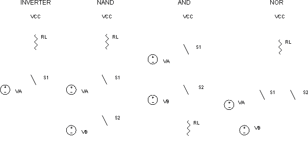
The described circuit focuses on simulating a NAND gate using SPICE switches to represent the functionality of NMOS transistors. The NAND gate is a fundamental digital logic gate that outputs a low signal (LO) only when both of its inputs (A and B) are high (HI). This behavior can be achieved by connecting two SPICE switches (S1 and S2) in series, which effectively implements the AND function. The output is inverted by a pull-up resistor (RL), which is connected to the power supply, thereby producing the NAND gate's characteristic output.
The circuit is defined as a subcircuit for ease of integration into larger designs. The nodes of the subcircuit are clearly specified, allowing for straightforward connections in various configurations. The simulation file, named LOGIC_SW.CIR, utilizes two binary signal sources, VA and VB, to generate input combinations (00, 01, 10, and 11) for testing the NAND gate's operation. A power supply of +5V (VCC) is provided to ensure adequate voltage levels for the logic gate's operation.
For visualization, the simulation allows plotting of the input signals (V(1) and V(2)) and the output signal (V(3)). A separate plot for V(3) can enhance clarity, particularly in observing the output's behavior when both inputs are HI. The resistance between switch nodes (R(3,5)) is defined to vary based on the input voltage levels, with specific resistance values assigned at different voltage thresholds (2.4V and 2.6V). This variable resistance feature allows for a more realistic simulation of the transition states between ON and OFF conditions.
It is essential to consider transient analysis challenges that may arise due to fast input transitions, particularly in more complex circuits that include feedback or feedforward paths. To mitigate potential simulation failures, it is advisable to introduce RC delay components to slow down the transitions, ensuring that the SPICE simulation can accurately compute results. Additionally, the finite rise and fall times of the input signals (V(1) and V(2)) should be factored into the analysis, as the output (V(3)) will respond rapidly when the inputs cross the defined logic threshold level, approximately 2.5V in this case. This behavior is crucial for understanding the dynamic operation of the NAND gate within the context of digital logic simulation.You're simulating a circuit, it requires several digital gates, but you don't have a mixed-mode simulator. What to do? One solution involves creating simplified versions of the logic functions. To do this, we look to the NMOS transistor implementation of logic gates where the transistor acts like a voltage-controlled switch.
But, instead of the transistor, we'll use the SPICE switch. Just like the transistor, the switch is defined to turn ON when the input voltage goes HI. So let's have a go at simulating the NAND gate. How do you describe its function? When both A and B are HI, the output is LO. Or stated another way - it's the AND function with an inverted output. The circuit appears below. S1 and S2 in series create the AND function; RL in the pull-up position inverts the output. Defining the NAND gate as a subcircuit makes it easy to insert it into a few locations if you wish. The subcircuit nodes are listed in parenthesis. Simulate the SPICE circuit named LOGIC_SW.CIR. VA and VB create two binary signals that form the sequence 00, 01, 10 and 11. VCC = +5V supplies power to the logic gate. Plot the inputs V(1), V(2) and the output V(3). For a clearer view, you might want to plot V(3) in a separate plot window. Does the output go LO when V(1) and V(2) are HI? Defining the term R(3,5) as the resistance between switch nodes 3 and 5, you can interpret the model as follows. If V(1,0) ? 2.6V then R(3,5) = 10 ?. Similarly, if V(1,0) ? 2.4V then R(3,5) = 1 M?. Between the ON and OFF voltages, 2.4V ? V(1,0) ? 2.6V, the resistance varies continuously between RON and ROFF. (Using RON, ROFF, you could define a switch that turns OFF when the input goes HI.) You could run into trouble when running a transient analysis on devices with fast transitions.
SPICE algorithms may fail under these conditions. This is especially true with complex circuits having feedforward or feedback paths. ( Like RS flip-flops created from NAND gates.) The solution is to sprinkle a little RC delay on the devices slowing the transitions enough to where SPICE successfully computes the simulation. Note the finite rise and fall times of V(1) and V(2). You may have also noticed that the output V(3) quickly changes when the inputs pass through 2.5 V. This is the approximate logic threshold level defined for the SPICE switches. 🔗 External reference
Related Circuits
This circuit provides a visual 9-second delay using a 7-segment digital readout LED. When the switch is closed, the CD4010 up/down counter is preset to 9, and the 555 timer is disabled with the output held high. When the...
This digital thermometer indicates the temperature measured with an NTC using 7 LEDs. The circuit works using an opamp, the well-known 741, which amplifies the voltage difference between its plus and minus input. This amplification (sensitivity) can be set...
This is a versatile digital counter circuit that is cost-effective due to the basic components available in many electronic shops. The digital counter circuit is designed to count pulses and display the count on a digital readout, typically using a...
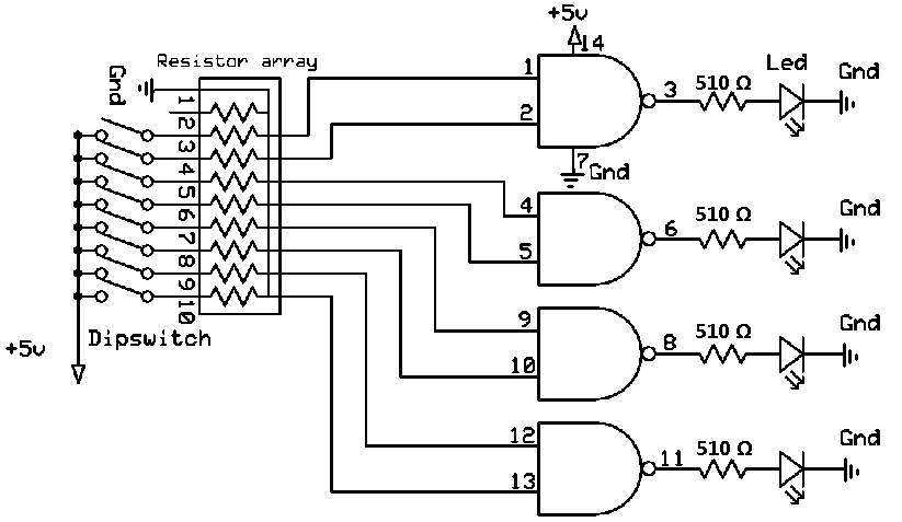
A Dual Inline Package (DIP) switch can be utilized to select between 0 and 5 volts in a circuit. Since the DIP switch lacks power or ground connectors, these must be provided externally. When the switch is in the...
This digital volume control has no pot to wear out and introduces almost no noise in the circuit. Instead, the volume is controlled by pressing UP and DOWN buttons. This simple circuit would be a great touch to any...
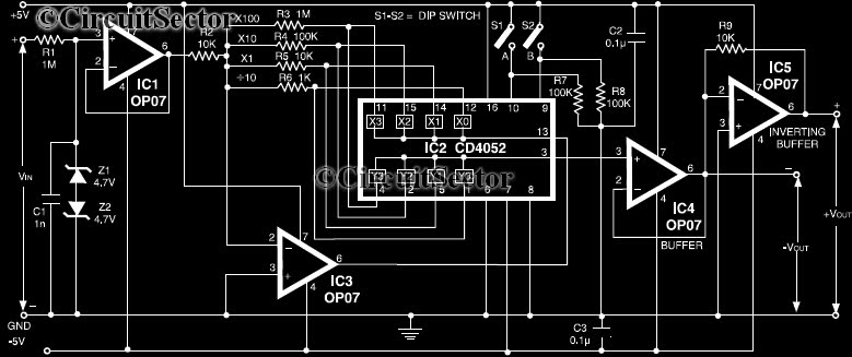
This circuit is a precision amplifier with digital control, designed for signal conditioning of low-output transducers operating in the millivolt range. The resistors R3 to R6 can be user-selected, with values ranging from 1 kilo-ohm to 1 mega-ohm, allowing...