
Driving a Capacitive Load with an H-bridge
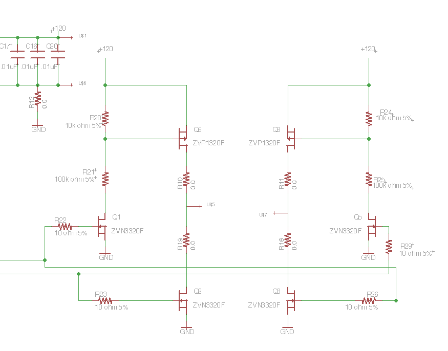
The circuit design involves a Class D amplifier that utilizes an H-bridge configuration to produce a square wave output suitable for driving an electroluminescent (EL) panel. The H-bridge is responsible for switching the voltage across the EL panel, allowing for the necessary alternating current to excite the phosphorescent material within the panel. The DC/DC boost converter is integrated to elevate the input voltage to the required +/- 120V, which is essential for the operation of the EL panel.
In this configuration, the output bypass capacitors play a critical role in stabilizing the voltage during transient load conditions. The bypass capacitors (C16, C17, C20) are strategically placed to provide immediate current supply when the load demands exceed what the flyback converter can deliver. The choice of capacitance values directly affects the response time and stability of the output voltage.
The EL panel's performance is influenced by its equivalent circuit model, which combines resistance and capacitance. The resistance decreases with increased frequency, indicating that at 1kHz, the expected load is primarily resistive at 56kΩ. However, the unexpected current draw of 360mA indicates that the panel's behavior under dynamic conditions may differ from the static measurements taken with the LCR meter.
The investigation into the voltage drop and current behavior suggests that the flyback converter's control mechanism may require adjustment to better handle sudden load changes. This could involve tuning the duty cycle response to accommodate rapid fluctuations in load, ensuring that the output voltage remains stable during operation.
Ultimately, the decision to enhance the bypass capacitance or redesign the power supply hinges on the desired performance characteristics of the EL panel. A balance must be struck between maintaining peak voltage for brightness and ensuring adequate current supply to prevent dimming during operation. The insights gained from this analysis will inform future design considerations and modifications to optimize the performance of the Class D amplifier and its associated components.Alright, so I had some post-publication weirdness following my last post, and it took me a few days to figure out exactly what was up, but I think I finally have all the details, and I learned a lot in the process. I noticed some weirdness towards the end of writing my 8, 000+ behemoth of a post last week. For those of you just checking in, I built a simple Class D amplifier to provide an EL panel with a +/- 120V square wave. A Class D is basically an H-bridge attached to a DC/DC boost converter. Here`s the schematic of my H-bridge along with the output bypass capacitance of my DC/DC flyback (boost) converter on the left. The two tabs in the middle connect to my EL panel: I spent most of the post designing my boost converter based on my expected load.
My load was an EL panel which I measured with an LCR meter and got the following: Based on some rudimentary research, I had assumed that an EL panel could be modeled as a resistor and capacitor in series. The resistance would drop as the frequency increased, but because I was planning on driving no faster than 1kHz, my load would primarily be a 56k as my desired load and did all my component sizing based on driving that steady load at 120VDC.
Once I finally put everything together though, I noticed that my positive rail wasn`t doing a very good job maintaining that 120V: Now, I had some explanation for this. My flyback converter was controlled by a special chip that tries to maintain the output voltage by controlling the duty cycle going into the flyback.
It`s possible that the flyback controller was simply not anticipating the sudden increase in load on the rail and therefore was unprepared when it hit. It was essentially going from an infinite resistance (fully charged capacitor) where it had probably dropped the duty cycle close to zero to a 56k Trying to confirm this theory, I took some measurements of the slope of the voltage drop figuring that because the flyback was basically shut off at this point, the only thing supplying current to the load were the bypass capacitors on the rail (C16, C17, C20 above).
Now, when I originally published the post, I found the initial voltage drop to be consistent with a 3. 6mA load which is about on par with what I was expecting for a 56k It was only after publishing did I realize that I was measuring with a voltage divider and forgot to convert back to real Volts!
This means that I wasn`t drawing 3. 6mA, I was drawing 360mA! This was completely impossible with a 56k So, I remarked in the last post that this problem could easily be solved by just adding more bypass capacitance. As it turns out this solution is correct. After adding a huge 4. 7 So it would appear from the video that a steadier rail actually makes the EL panel dimmer. It looks like in this situation, my panel benefits more from a higher voltage peak than from a steadier rail.
My larger capacitor is averaging the ripple, and at this frequency, my power supply can`t keep up with the current draw. The average voltage is actually much lower than the peak. This leaves me with two options. I can either leave the power supply how it is and accept a slightly dimmer panel, or I can redesign it from the ground up to make it better.
I might end up doing both, but that`s a project for the future. For the present, my only concern is better understanding the problem. I had measured the R and C with the LCR meter, and was convinced that I was right figuring that the energy dissipated in the resistor was the energy you see as light. The idea is that an EL panel consists of three parts. There is a phosphorescent material in the middle, and it`s sandwiched between two layers of insulator.
At low voltage, each layer acts like a capacitor in series with the others. This is probably the capacitance I was reading with the LCR meter. 🔗 External reference
Related Circuits
For a project such as a robot or car, an electronic circuit is required, controlled by a control circuit. This control circuit outputs signals to manage an H-Bridge. The circuit includes a Hex Bug design, where the control circuit...
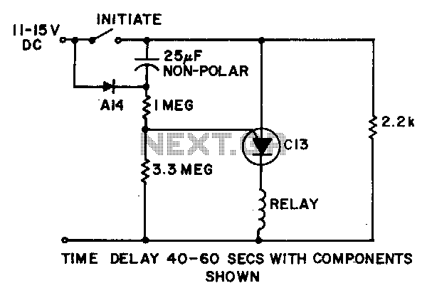
Power is applied to the circuit with the initiate switch open. The 25 µF capacitor charges through the A14 diode, or an equivalent, and a 2.2 kΩ resistor to the full supply voltage. When the initiate switch is closed,...
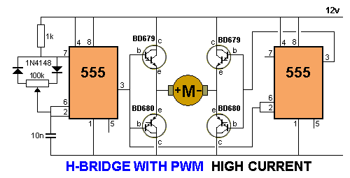
The following circuit illustrates an N-Channel H-bridge motor drive circuit diagram. Features include low voltage motor drives utilizing N-channel MOSFETs. The N-Channel H-bridge motor drive circuit is designed to control the direction and speed of a DC motor using low...
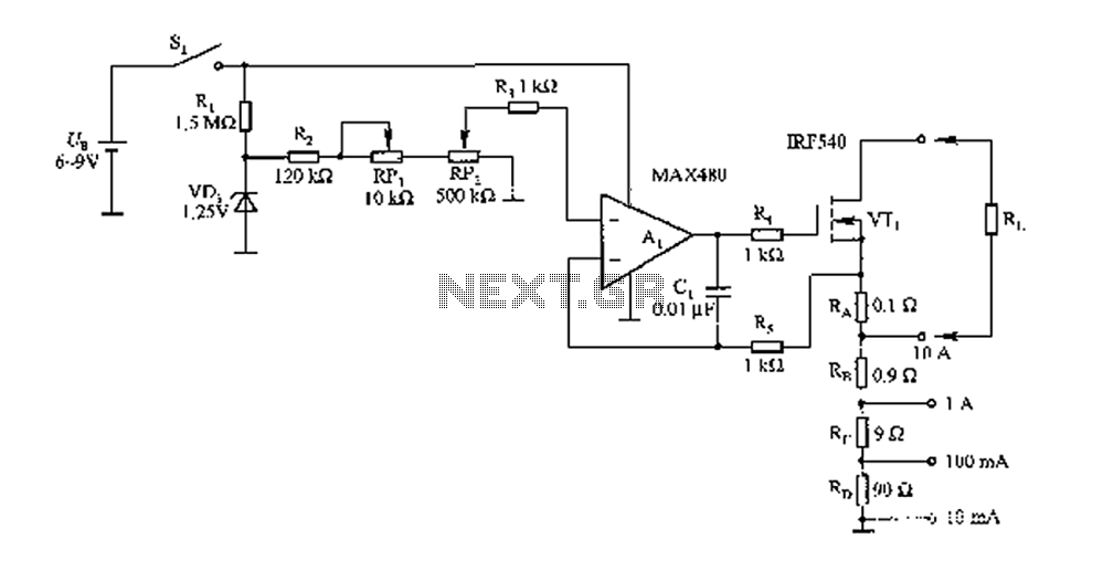
The FIG load test is a control circuit designed for external loads up to 10A, commonly utilized in drive test power applications, power amplifiers, LED solenoids, and relays. It is capable of handling various resistive loads and features a...
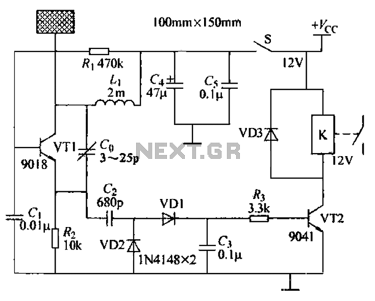
A capacitive proximity controller typically consists of a radio frequency oscillation circuit and a detection plate. The circuit is constructed using discrete components for capacitive proximity sensing detection. The transistor VT1, along with surrounding components, forms a radio frequency...
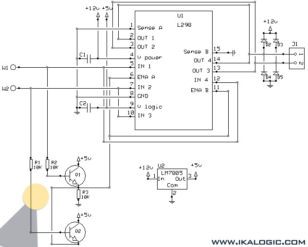
This implementation utilizes the L298 integrated circuit to drive motors and inductive loads with a continuous current capacity of up to 4A. The L298 consists of two independent channels, each capable of driving loads of up to 2A. By...