
Heavy duty battery charger
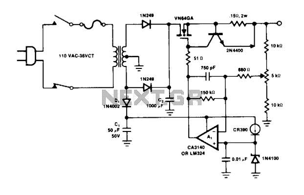
The circuit operates by utilizing an operational amplifier (op-amp) configuration where A1 functions as an error amplifier, comparing the output voltage against a reference voltage provided by the zener diode. The VN64GA, a voltage regulator, is driven by the error signal to maintain the desired output voltage level. The design incorporates a peak rectifier D1, which is essential for converting the AC input into pulsating DC, and capacitor C1, which smooths the rectified output to provide stable voltage levels to the op-amp and zener reference.
The additional drive voltage requirement for the VN64GA ensures that it can operate efficiently under full load conditions. This is particularly significant for applications such as battery charging, where a stable output is crucial. The increased capacitance of C2 enhances the filtering capability, allowing for a more regulated output, while the addition of another electrolytic capacitor across the load further stabilizes the voltage and reduces ripple.
The 2N4400 current limiter is a protective feature that prevents excessive current draw, safeguarding the circuit components. It is designed to limit the output current to a maximum of 4.5 A. However, caution is advised, as prolonged short-circuit conditions can lead to thermal overload of the VN64GA. Therefore, a heat sink with a thermal resistance of approximately 1°C/W is recommended to dissipate heat effectively and maintain safe operating temperatures.
In summary, this circuit design effectively combines an operational amplifier, voltage regulator, rectification, and current limiting to create a reliable power supply system suitable for battery charging and other applications requiring regulated DC output. The careful selection of components and their configuration ensures fast response times and thermal management, making the circuit both efficient and robust.Operation amplifier A1 directly drives the VN64GA with the error signal to control the output voltage. Peak rectifier Dl, CI supplies error amplifier A1 and the reference zener. This extra drive voltage must exceed its source voltage by several volts for the VN64GA to pass full load current.
The output voltage is pulsating dc which is quite satisfactory for battery charging. To convert the system to a regulated dc supply, capacitor C2 is increased and another electrolytic capacitor is added across the load. The response time is very fast, being determined by the op-amp. The 2N4400 current limiter circuit prevents the output current from exceeding 4.5 A. However, maintaining a shorted condition for more than a second will cause the VN64GA to exceed its temperature ratings. A generous heat sink, on the order of 1°C/W, must be used. 🔗 External reference
Related Circuits
The concept involved removing the center page from a magazine and cutting it into four pieces to create a card suitable for a filing system. The front side of each card provided connections to the integrated circuit (IC), while...

This design is for a charger circuit suitable for lead-acid batteries, including flooded, gel, and AGM types. The circuit features a simple design. The automatic function means that this charger will stop charging automatically when the battery voltage reaches...
Widely available AA NiMH battery chargers are on the market, including those packaged to charge various battery types such as NiCd and NiCad. This project features a battery charger designed for two AA NiMH or NiCd cells of any...
A simple NiCd charger can be constructed using commonly available components and an inexpensive LM317 or 78xx voltage regulator. It incorporates a current limiter made up of resistor R3 and a transistor, allowing it to charge multiple cells until...

After experiencing equipment failure, a decision was made to replace a combination inverter/charger unit with individual components that fulfill the same requirements. The combination unit, referred to as the "Everything Box," is an efficient solution for cost savings by...

This circuit displays three voltage levels: normal (11 to 15 V), high (greater than 15 V), and low (below 11 V). When the voltage is low, the LED illuminates steadily. In the normal voltage range, the LED remains off....