
HV REGULATOR WITH FOLDBACK CURRENT LIMITING
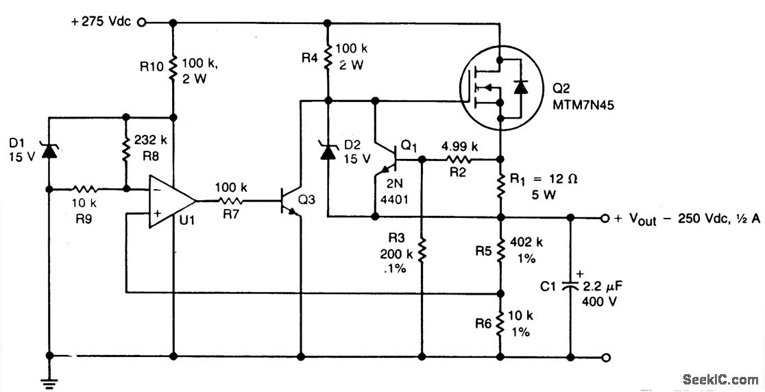
The circuit employs a TMOS MTM7N45 transistor as the primary series pass element in a linear high voltage power supply configuration. The design is capable of accepting an unregulated input voltage of +275 V and regulating it down to a stable output voltage of 250 V. This regulation is crucial for applications requiring precise voltage levels, especially in high-voltage environments.
The operational amplifier U1 plays a significant role in maintaining the output voltage by comparing a fraction of the output voltage to the reference voltage provided by the 15 V zener diode D1. This feedback mechanism ensures that the output remains stable despite variations in load or input voltage. The operational amplifier's output is connected to the base of transistor Q3, which acts as a driver for the gate of the TMOS MTM7N45. This arrangement allows for efficient control of the pass element, enabling it to adjust its conduction based on the feedback received.
To enhance the reliability of the power supply, foldback current limiting is incorporated into the design. This feature prevents excessive current from flowing through the pass element, thereby protecting both the circuit and the load. The foldback current limiting circuit consists of resistors R1, R2, R3, R4, transistor Q1, and diode D2. These components work together to sense the output current and adjust the gate voltage of the TMOS MTM7N45 accordingly. The limiting action is characterized by a "knee" in the current output, which can be calculated using a specific formula that defines the threshold at which the current limiting begins to take effect.
Overall, this high voltage linear power supply design exemplifies a robust approach to voltage regulation and current limiting, ensuring that the output voltage remains stable and safe for connected loads, while also protecting the circuitry from potential damage due to overcurrent conditions.A TMOS MTM7N45 (Q2) is used as a series pass element in a linear high voltage supply that accepts +275-V unregulated and produces 250 V regulated with foldback current limiting. A 15-V zener, D1, provides the dc reference for operational amplifier U1, whose other input is obtained from a fraction of the output voltage.
UI drives Q3, which drives t he gate of Q2. Foldback current limiting is achieved by RI, R2, R3, R4, Q1, and D2. The formula to estab!ish the current "knee" for limiting is: 🔗 External reference
Related Circuits
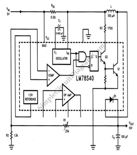
A step-up conversion can be achieved without utilizing a transformer. This circuit is capable of converting a 5V DC source into 15V. It is important to note that there is no power gain. The described circuit employs a DC-DC boost...
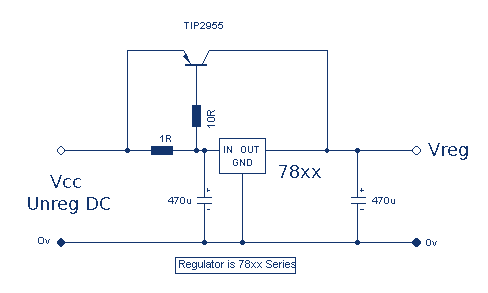
Although the 78xx series of voltage regulators are available with different current outputs, you can boost the available current output with this circuit. A power transistor is used to supply extra current to the load, maintaining a constant voltage....
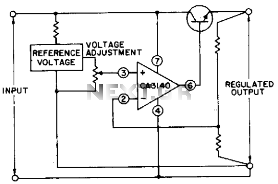
The circuit utilizes a CA3140 BiMOS operational amplifier that is capable of providing a regulated output adjustable from approximately 0 to 24 volts. The circuit is fully regulated. The CA3140 BiMOS operational amplifier is a versatile component that combines the...
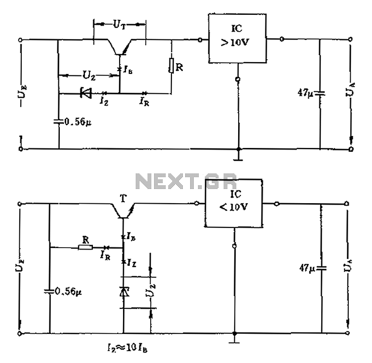
The voltage equation Ue = Ut + Ur + Ua indicates that the transistor voltage Ut will determine the maximum output voltage Ua. Additionally, Ur must be 2V. The voltage regulator's voltage value depends on the selection of Uz....
The current loop interface is widely used in industrial environments due to its robustness. Its noise resistance and failure detection capabilities make it suitable for various applications. The current loop interface, commonly referred to as a 4-20 mA current loop,...

This circuit requires a control current that is 100 times smaller than that required by standard optically isolated solid-state relays. It is particularly suitable for battery-powered systems. By utilizing a combination of a high-current TRIAC and a very sensitive...