
LAN Tester circuit diagram
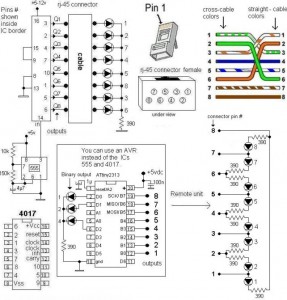
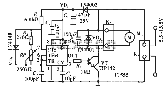
The first design of the LAN tester circuit incorporates the 555 timer IC configured in astable mode to generate a pulse signal. This pulse signal is fed into a decade counter, specifically the CD4017, which counts the pulses and activates the corresponding output pins sequentially. The outputs can be connected to LEDs or other indicators to display the status of the LAN connections. The use of the 555 timer allows for adjustable timing intervals, providing flexibility in how the tester operates. The decade counter's outputs can be used to indicate various conditions such as link status or signal integrity.
The second design employs the ATtiny2313 microcontroller, which offers a more sophisticated and programmable approach to LAN testing. This microcontroller can be programmed to perform a variety of tests, including checking for continuity, measuring signal quality, and providing detailed diagnostic information through a serial interface or LED indicators. The microcontroller's versatility allows for more complex logic and the ability to adapt to different testing scenarios, making it suitable for advanced users who require detailed feedback on network performance.
Both designs serve the essential function of testing LAN connections, but they cater to different levels of complexity and user requirements. The choice between the two designs depends on the specific needs of the user, whether a simple and straightforward testing method is required or a more advanced, programmable solution is preferred.LAN tester circuit diagram provided in two designs. The first design use timer IC 555 and decade counter 4017. The second design use microcontroller ATtiny2313 🔗 External reference
Related Circuits
The completed board may be driven by voltages between 0.8 and 3 Volts. While the basic design goal was candle-like light from a single cell, the values used were chosen to allow safe operation from 3 Volts so you...
Depressing SI charges CI to the supply voltage. This biases Q1 on via bias resistors R2 and R3. A voltage is available for the duration of the delay period to hold off the alarm circuit. CI can be increased...
The circuit illustrated in Figure 2-49 is straightforward, featuring a cold Positive Temperature Coefficient (PTC) thermistor element. It utilizes the thermal resistance characteristics of the lamp to manage the delay time, which typically ranges from 10 to 30 seconds....
The circuit operates using pulse position modulation, which is a method distinct from the more commonly utilized pulse width modulation for speed control. A 555 timer is employed as a square wave modulator, generating output pulses with a fixed...
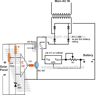
The automatic changeover relay circuit was requested by Mr. Karimulla Baig. The circuit is designed to charge a connected battery at a constant current using power from a solar panel. In the absence of solar energy, such as during...
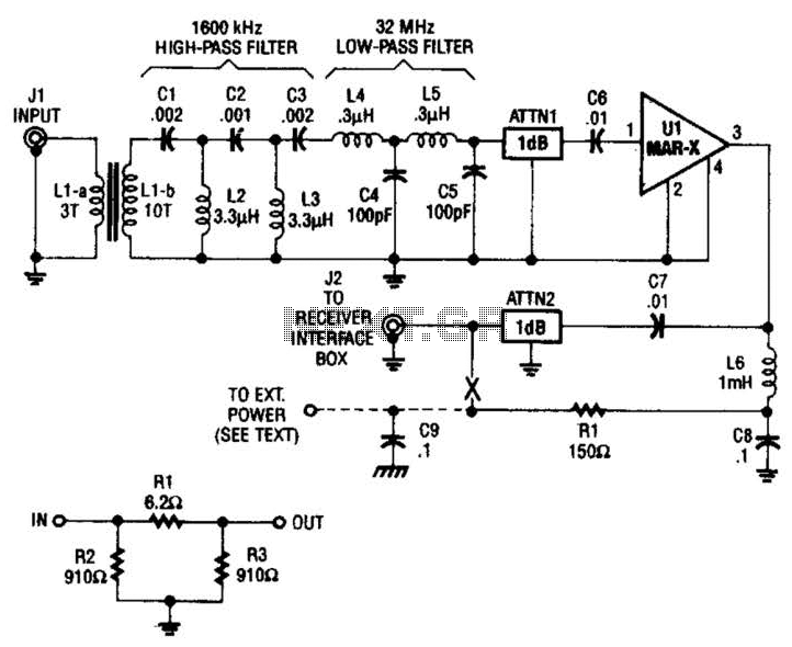
The HF/SW receiver preamplifier consists of a broadband toroidal transformer (LI-a and Ll-b), an LC network featuring a 1600-kHz high-pass filter and a 32-MHz low-pass filter, inductors L2 and L3 (26 turns of #26 enameled wire wound on an...