
laser diode driver circuit
The laser diode driver circuit utilizes a voltage-controlled current source architecture to deliver precise current to the laser diode, ensuring optimal performance and longevity of the diode. The OPA350 operational amplifier, known for its low offset voltage and high precision, is employed in a rail-to-rail configuration to maximize output swing and drive capability.
The Howland current pump configuration is particularly advantageous in this application due to its ability to provide stable current output regardless of load variations. The inclusion of Q1 as a current booster enhances the output drive capability, allowing for higher currents to be delivered to the laser diode while maintaining linearity and minimizing distortion.
The shunt resistor (RSHUNT) is strategically placed in series with the laser diode to enable accurate current sensing. By measuring the voltage drop across this resistor, the circuit can determine the actual current flowing through the diode, facilitating feedback control. This feedback loop is crucial for maintaining the desired current level, especially in applications where the diode characteristics may change with temperature or aging.
The control input (VIN) can be adjusted using an analog voltage from a potentiometer or a digital-to-analog converter (DAC) controlled by a microprocessor. This flexibility allows for easy integration into automated systems or manual adjustments, providing versatility in various operational scenarios.
The design achieves a scale factor of 1V input to 1A output, making it straightforward to calculate the required input voltage for a specific desired output current. This linear relationship simplifies the design process for applications requiring precise control over laser diode operation, such as in optical communication systems, laser cutting, or medical devices.
Overall, this laser diode driver circuit is characterized by its simplicity, precision, and reliability, making it an excellent choice for applications demanding high-quality laser performance.This is circuit design for a laser diode driver can be implemented using voltage-controlled current source. This simple linear laser diode driver gives cleaner drive current than a switched (PWM) drivers. This circuit is based on OPA350 IC. This is the figure of the circuit. A Howland current pump with a current booster is used as the basic of thi s laser diode driver. Q1 is used as the current booster on the output of a R-R CMOS OPA350 op amp (U2). Voltage drop across a shunt resistor (RSHUNT) in series with the laser diode is measured differentially to sense the current. An analog voltage from a potentiometer of from a microprocessor controlled DAC can be fed to VIN to control the laser diode current.
Using the component values as shown, the scale factor is 1V input equals 1A output. 🔗 External reference
Related Circuits
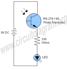
This is a straightforward infrared detector circuit designed to detect infrared light. The circuit comprises only three components: an RS-276-145 photo transistor, a 330-ohm resistor, and a general-purpose LED (Light Emitting Diode). When the photo transistor receives infrared light...
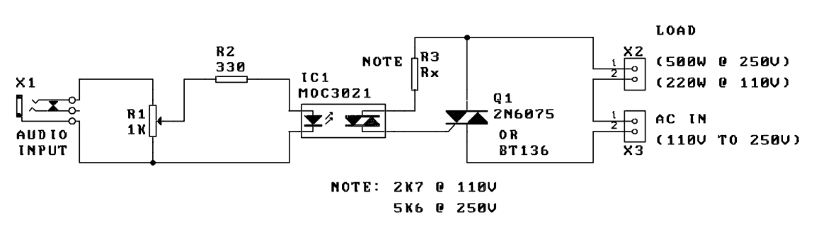
A music-to-light modulator is a circuit which controls the intensity of one or more lights in response to an audio input. The problem in older circuits is that there was a direct electrical connection between the lights using mains...
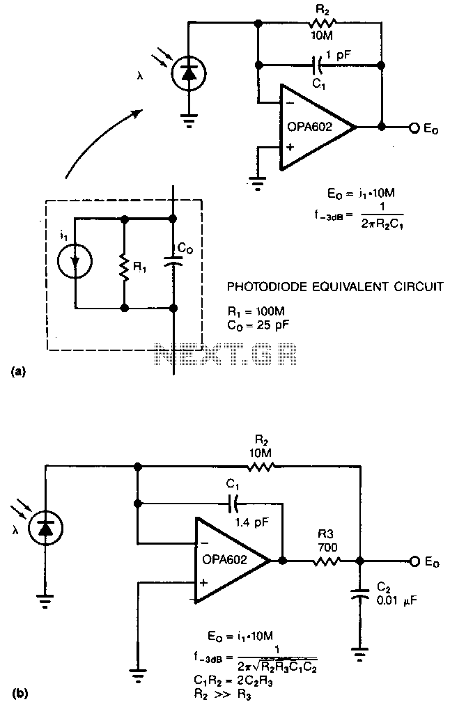
Adding two passive components to a standard photodiode amplifier reduces noise. Without the modification, the shunt capacitance of the photodiode reacting with the relatively large feedback resistor of the transimpedance (current-to-voltage) amplifier creates excessive noise gain. The improved circuit...
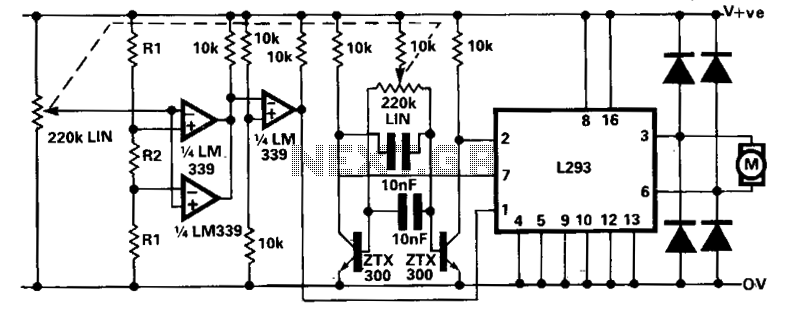
A limitation of the bi-directional proportional motor control circuit is that when the potentiometer is in its center position, the motor does not stop but continues to creep. This occurs due to the challenge of precisely adjusting the potentiometer...
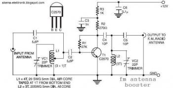
The input coil L1 is composed of four turns of 20 SWG enamelled copper wire, wound slightly spaced over a 5 mm diameter former. It is tapped at the first turn from the ground lead side. Coil L2 is...
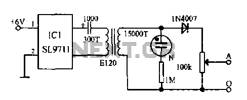
The electronic frostbite treatment instrument ASIC SL9711 consists of an oscillation circuit, a power amplifier, and a controller. It generates a sine wave at frequencies of 100 Hz and 3 Hz, followed by a step-up transformer with potentiometer adjustment...