
Light Sequencer Circuit

The light sequencer circuit operates by utilizing the timing capabilities of the 555 timer, which is set up in an astable mode. This configuration allows for continuous oscillation, generating a square wave output that serves as a clock signal. The frequency of this square wave is adjustable, providing flexibility in the timing of the light sequencing. The capacitors and resistor in conjunction with the potentiometer allow for fine-tuning of the pulse width and frequency, enabling the user to customize the light display according to their requirements.
The 4017 Johnson counter is a decade counter that counts from 0 to 9. It provides a high output on one of its ten pins sequentially with each clock pulse received from the 555 timer. This sequential output is essential for controlling the SCRs, as each SCR corresponds to a specific output pin on the 4017. The resistive coupling between the output pins and the SCR gates ensures that the SCRs are triggered appropriately, allowing for the controlled illumination of the connected lamp.
The inclusion of a fuse in the power supply circuit is a critical safety feature, protecting the circuit from overcurrent conditions that could lead to damage. The conversion of AC to pulsating DC by diode LD1 is crucial for the operation of the SCRs, which require a specific polarity to conduct. The smoothing capacitors C2 and C3 help to reduce the ripple in the pulsating DC, providing a more stable voltage for the subsequent stages of the circuit.
Resistor R23 plays an important role in current limiting, ensuring that the SCRs are not subjected to excessive gate current, which could lead to failure. The zener diode D2 serves as a voltage regulator, maintaining a consistent output voltage of 6 VDC, which is important for protecting sensitive components in the circuit from voltage spikes. Overall, this light sequencer design effectively combines timing, control, and safety features to create a functional and reliable lighting sequence. The light sequencer uses two ICs and 10 SCRs to create.an ac sequencer. The first 10, a 555 timer, is used to provide clock pulses for 102. The 10 is configured as an astable multivibrator, and its output is on pin 3. Capacitors CI and 04, along with resistor R2 and potentiometer PI, control the frequency of the pulses. IC2 is a 4017 Johnson counter, which shifts a high-signal level to each one of its 10 output pins in sequence.
Each output pin is resistively coupled to the gate lead an an SCR. When the respective output pin on the 4017 is high and the positive half of the ac cycle is on the anode lead of the SCR, it turns on. The lamp that is connected to its anode lights. Power is brought into the PC board by the line cord, then the circuit is fuse-protected. Diode LD1 changes the ac to pulsating, which is smoothed by C2 and C3. R23 limits the current, and zener diode D2 limits the dc voltage to 6 Vdc.
Related Circuits
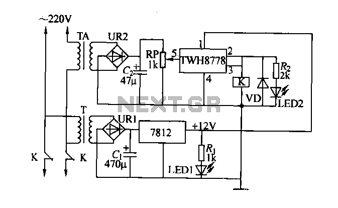
An electric power limiter circuit restricts the user load, ensuring that household appliances operate within a specified normal current range. When the load exceeds a predetermined threshold, the power supply is disconnected. This circuit utilizes the high-power integrated TWH8778...
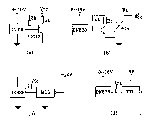
Figures (A), (B), (C), and (D) illustrate outputs that can directly drive transistors, thyristors, relays, CMOS circuits, and TTL circuits. The described figures depict various output configurations capable of interfacing with different electronic components. Each output is designed to provide...
Circuit stereo TDA2822 audio power amplifier circuit schematics. In this series, the TDA2822M IC is utilized as the primary amplifier. Additionally, alternatives such as KA2209 and NJM2073 can also be employed. The TDA2822 audio power amplifier circuit is designed to...
The diagram illustrates a series connection of cell diode capacitors, each rated for an increasing voltage of 300 V. This configuration generates a high DC voltage supply of 40 kV, which can be utilized for various experimental applications. With...
This circuit is designed to control the mains voltage by switching it on and off at intervals ranging from just under a second to up to 10 minutes. It is particularly useful for testing mains-operated equipment over extended periods...
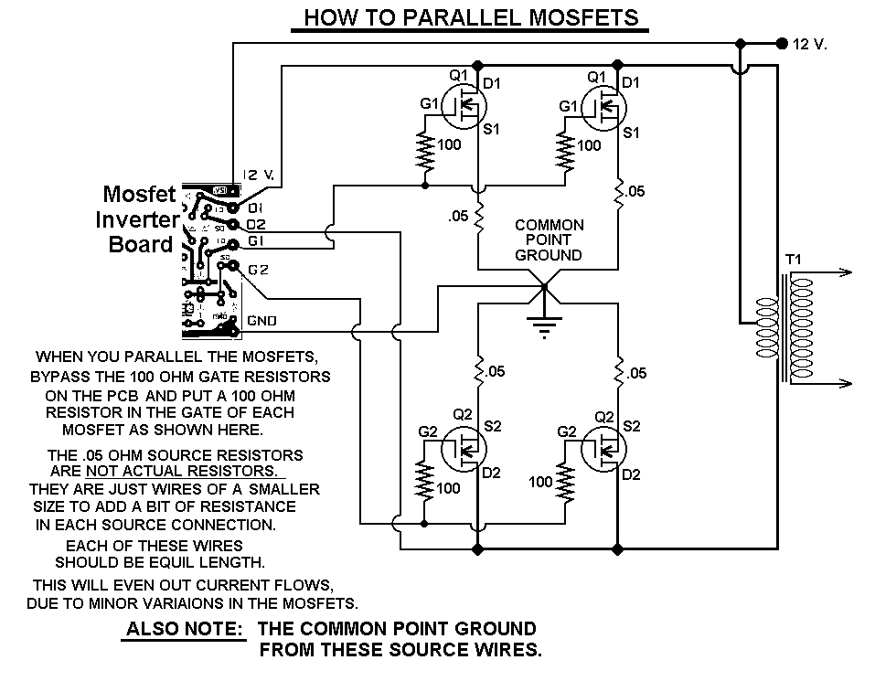
This 1000-watt power inverter circuit diagram is based on the MOSFET RF50N06. For increased power output, additional MOSFETs can be paralleled with the RF50N06. These MOSFETs are rated for 60 volts and 50 amps. It is essential to connect...