
Low drift integrator
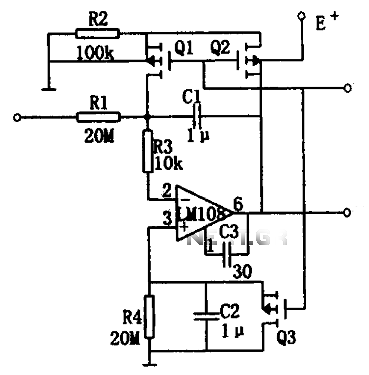
The described integrator circuit features a high degree of stability and low drift characteristics, making it suitable for precision applications across a wide temperature range. The core components include an operational amplifier, which serves as the primary active element, along with passive components such as resistors and capacitors that define the integrator's time constant and stability.
In the basic configuration, the operational amplifier's inverting and non-inverting inputs are strategically utilized to manage the integration of input signals. The addition of resistor R4 and capacitor C2 at the non-inverting input helps mitigate the effects of input bias currents, which can introduce unwanted offset voltages that affect circuit performance. By ensuring that R4 matches R1 and C2 matches C1, the circuit can maintain balance, further reducing drift.
The reset mechanism, implemented through FETs Q1 and Q2, plays a critical role in maintaining the integrity of the integrator function. When activated, these FETs effectively short-circuit capacitor C1, allowing any accumulated charge to dissipate. This action prevents the input bias current from generating an offset voltage during the reset phase, ensuring that the circuit can start from a known state without residual voltages affecting subsequent measurements.
The operational amplifier’s configuration allows for the integration of signals while maintaining the ability to counteract any offset voltages that may arise. This is achieved by utilizing feedback mechanisms that stabilize the output against variations in input conditions. The use of the LM108 operational amplifier is particularly advantageous due to its high input impedance, which minimizes loading effects on the signal source and enhances overall circuit performance.
Overall, this integrator circuit design is well-suited for applications requiring high precision and stability, particularly in environments subject to temperature variations. By carefully selecting component values and configurations, the integrator can achieve reliable performance with minimal drift, making it an essential component in various electronic systems. As shown in FIG integrator drift is very small, at a temperature of -55 C ~ + does not exceed 500 V/s within 125 C range. FIG basic integrator constituted by an operational amp lifier, resistor R1 and capacitor C1. In order to improve the stability of the integrator, the circuit in the operational amplifier non-inverting input plus a resistor R4 and capacitor C2 (R4 R1, C2 C1), the input bias current points. Reset circuit, the FET Q1 and Q2 short-circuiting the capacitor C1, R1 flowing through the input bias current will not cause the offset voltage.
When Q1 and Q2 is turned off, the circuit start points, then the bias current flowing through R1 will produce offset voltage. In the same phase of the operational amplifier being connected to the integrating circuit can offset the offset voltage at the inverting input terminal generated.
When the two input bias resistors are equal, the output drift is very small. LM108 circuit used in a high input impedance operational amplifier.
Related Circuits
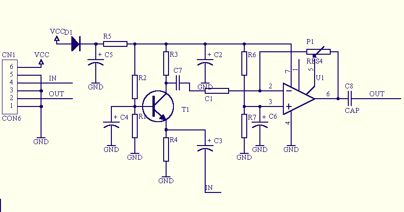
The circuit is a microphone amplifier for use with low impedance (~200 ohm) microphones. It will work with stabilized voltages between 9-30VDC. If you don`t build the impedance adapter part with T1, you get a micamp for higher impedance...
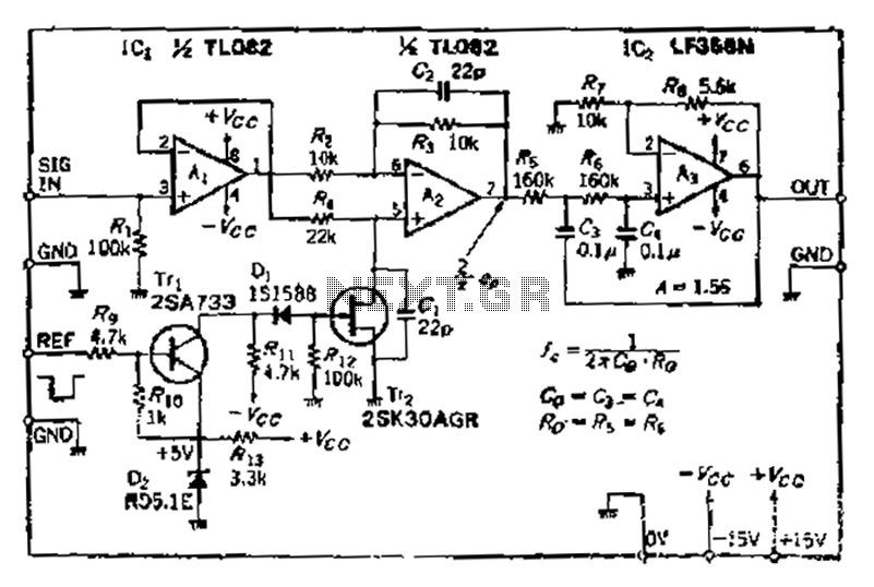
After turning off TT2, the input signal enters through chi Az, where the input resistance is very high and reaches the same potential. The inverting input terminal must also be associated with this movement. Therefore, Trr functions as a...
This circuit functions as a low-frequency warning device. The output from the oscillator generates a square wave signal, which is utilized to operate lamps or small relays. The circuit alternately flashes two incandescent lamps. The low-frequency warning device circuit typically...
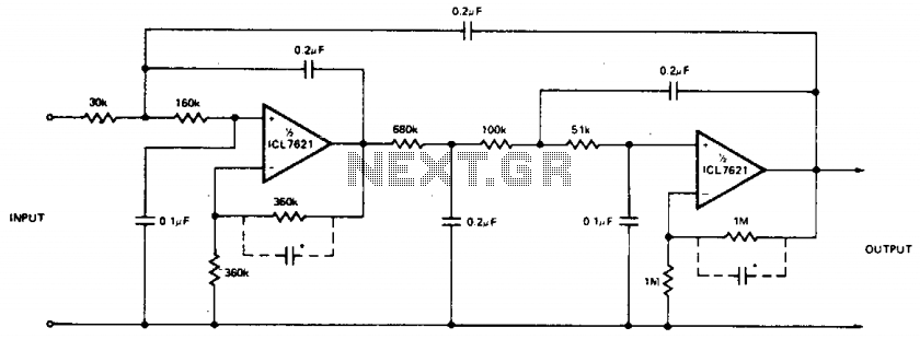
The low bias currents allow for the utilization of high resistance and low capacitance values, facilitating a low frequency cutoff at fc = 10 Hz, with an AVCL of 4 and a passband ripple of 0.1 dB. Additionally, small...
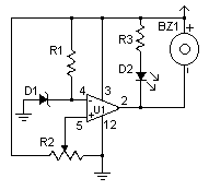
This low voltage circuit can be used to monitor batteries and other volatile sources of current for problems. The circuit sounds an alarm and lights an LED, but can be interfaced to any number of other circuits for many...
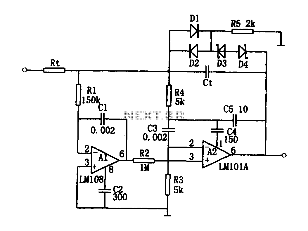
The high-speed integrating circuit is designed with an integration time constant circuit, RtCt, which offers a wide range. When the integrating capacitor Ct is not considered, A2 functions as a positive feedback compensation broadband AC amplifier. The negative feedback...