
NE555 Basic Monostable
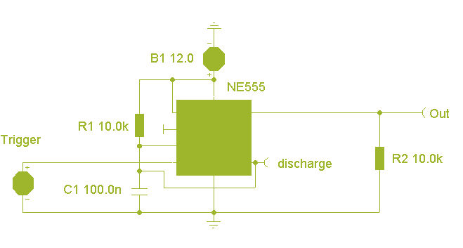
The 555 timer IC is a versatile component widely used in various timing applications. In a monostable configuration, the 555 timer produces a single output pulse in response to a triggering event, making it suitable for applications such as pulse generation, timer circuits, and delay circuits.
In this configuration, the timing period (T) is determined by the resistor (R1) and capacitor (C1) values according to the formula T = 1.1 x R1 x C1. The output pulse width can be adjusted by changing the values of R1 and C1, allowing for precise control over the timing interval. For instance, if R1 is set to 10 kΩ and C1 to 100 nF, the output pulse duration would be approximately 1.1 milliseconds.
The output of the 555 timer in monostable mode is a buffered signal, capable of interfacing directly with CMOS or TTL logic families. This characteristic ensures compatibility with various digital circuits, provided that the supply voltage levels are consistent with the requirements of the connected logic devices.
The timing diagram associated with this configuration illustrates the relationship between the trigger input, the output pulse, and the discharge terminal of the IC. When a negative-going trigger pulse is applied to the trigger pin (pin 2), the output (pin 3) transitions high for the duration specified by the timing period. After this period elapses, the output returns to its low state, and the discharge pin (pin 7) is activated to discharge the timing capacitor, preparing the circuit for the next triggering event.
Overall, the monostable configuration of the 555 timer is a fundamental building block in electronic design, offering simplicity and reliability in generating precise timing signals.Here the popular 555 timing IC, is wired as a monostable. The timing period is precise and equivalent to:- 1.1 x R1 x C1 With component values shown this works out at approximately 1.1msec.The output duration is independant of the input trigger pulse, and the output from the 555 is buffered and can directly interface to CMOS or TTL IC`s, providing that the supply voltages match that of the logic family. The timing diagram above shows the output pulse duration, the trigger input and the output at the discharge terminal of the IC. 🔗 External reference
Related Circuits
An automatic electric furnace temperature controller is illustrated. The closed circuit consists of a temperature detection output control loop; as the temperature increases, the output voltage rises until it reaches a preset temperature value, at which point the output...
In this project, an ATMEGA16 microcontroller operating at 16MHz will be utilized. To distinguish this project from others, a unique feature has been incorporated: a battery monitoring system. Many robots operate on new or freshly recharged batteries, and if...
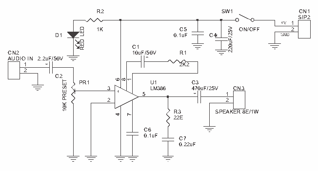
The Tiny Audio Amplifier kit is a good choice for battery operation. It is based on LM386 IC. Power supply - 6 - 12 VDC. Output power - 1 W, 8 Ohm. The quiescent power drain is only 24...
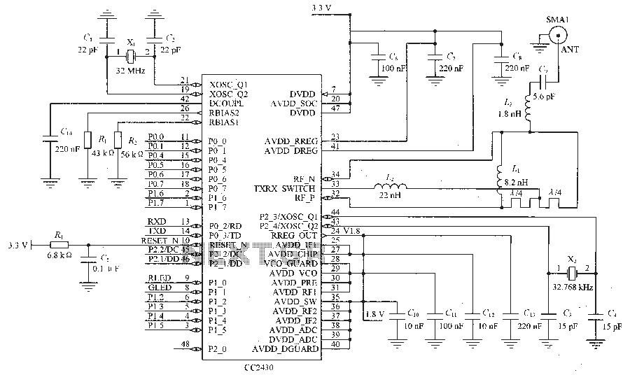
Figure C1 and C2 depict a 22 pF capacitor connected to a 32 MHz crystal oscillator circuit, which utilizes a quartz crystal for standard operation. Capacitors C3 and C4, each rated at 15 pF, are connected to a 32.768...
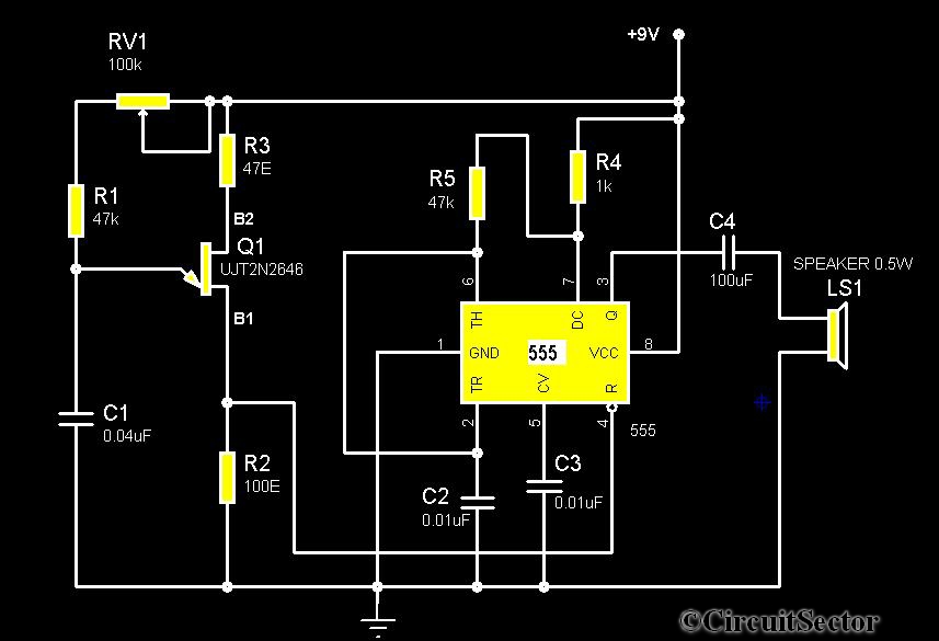
The circuit diagram illustrates a timer 555-based rain sound generator. It requires a 9V DC power supply, which can be provided by a 9V battery. The circuit utilizes a 0.5W, 8-ohm speaker to produce sound. When powered by a...

The utility vehicle anti-theft alarm circuit consists primarily of two main components essential for its operation. The security circuit is activated when the vehicle owner departs from the vehicle, utilizing an anti-theft switch (S B) to engage the alarm...
Warning: include(partials/cookie-banner.php): Failed to open stream: Permission denied in /var/www/html/nextgr/view-circuit.php on line 713
Warning: include(): Failed opening 'partials/cookie-banner.php' for inclusion (include_path='.:/usr/share/php') in /var/www/html/nextgr/view-circuit.php on line 713