
PSK transceiver circuit
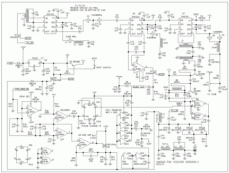
The transmitter utilizes another SA612 for mixing the BFO oscillator with a 9 MHz VXO signal generated by the SA612. The VXO consists of two crystals in parallel for an extended frequency range, complemented by a series inductor. The frequency is voltage-tuned using a 10-turn potentiometer and a 1N4756 Zener diode, which provides sufficient capacitance variation to tune the VXO by approximately 1.5 kHz, utilizing HC-49US crystals. This tuning range closely matches the bandwidth of the receiver's crystal filter.
The output from the transmitter mixer is filtered through a double-tuned circuit using modified 10.7 MHz IF cans. The modification involves breaking out the capacitor within the can, allowing it to be retuned to 14 MHz with an external capacitor. A two-stage transistor amplifier increases the signal level to drive the gate of a 74HC86 XOR gate. The XOR gate alters the phase of the transmitted signal and drives the gates of three BS170 MOSFETs used in the power amplifier, with two gates connected in parallel to enhance the drive capability.
During transmission, the PSK audio signal from the PC first enters a peak detector. A resistor across the peak detector's holding capacitor introduces some ripple, enabling the detector to track the modulation signal during the signal's falling edge. This ripple is subsequently filtered out by a low-pass filter. The resulting amplitude-modulated signal is then amplified in both voltage and current to power the RF power amplifier.
A voltage comparator is employed to detect zero crossings of the amplitude-modulated signal from the low-pass filter stage. The comparator's output clocks a "D" flip-flop, which is used to modify the phase of the transmitted signal via the 74HC86 driving the power amplifier.
The transmit condition is detected by sampling a signal from the AM modulation output transistor, which generates a sufficient level to activate a 2N7000 MOSFET. The output from this MOSFET mutes the audio output to the PC, disconnects the receiver input from the transmitter low-pass filter, and powers the transmit circuits through a PNP transistor switch.
A 4049 hex inverter produces a negative supply voltage for the operational amplifiers, preventing clipping on the negative swing of the input signal. An additional configuration of two diodes and capacitors creates a voltage doubler, enhancing the voltage available to supply the VXO tuning potentiometer and extending the VXO's tuning range. Although silicon 1N4148 diodes are illustrated in the schematic, using Schottky diodes such as 1S101 or 1N5811 may yield a higher output voltage.
A 78L05 three-terminal voltage regulator supplies a regulated voltage to most of the circuit components.The receiver is a basic SA612 circuit. (U5 and U6) The LO for 20 meters is about 9 MHz and an IF of 5.068 MHz. The IF filter uses two crystals and has a peak response at about 5.070 MHz, so this matches up well with the 20 M PSK sub-band centered at about 14.071 MHz. The BFO frequency is adjusted to be below the IF frequency so Upper Side Band reception results. This was done because it was easier to pull the transmitter VXO higher than the receiver LO frequency to get the proper beat notes in the audio band than it was to go the other way around.
The detected audio output of the BFO mixer is amplified by a simple LM386 amplifier (U2).
The transmitter uses another SA612 (U6) for mixing the BFO oscillator with a 9 MHz VXO signal produced by the SA612. The VXO uses two crystals in parallel for increased range, along with a series inductor. The frequency is voltage tuned using a 10 turn pot and 1N4756 Zener didoe used as a tuning diode, which gives enough capacitance swing to tune the VXO about 1.5 kHz, using HC-49US crystals.
This tuning range matches the band width of the receiver's crystal filter pretty closely.
The transmitter mixer output is filtered by a double tuned circuit, using modified 10.7 MHz IF cans. The modification is simply breaking out the cap in the bottom of the can, so it can be retuned to 14 MHz using an external cap.
A two stage transistor amp (Q4, Q6) brings the signal level up enough to drive the gate of a 74HC86 XOR gate (U4). The XOR gate is used to change the phase of the transmitted signal and to drive the gates of the three BS170 MOSFETs used for the power amplifier.
Two gates are connected in parallel to improve drive to the PA gates.
During transmit, the PSK audio signal from the PC first goes into a peak detector (U4a). A resistor across the peak detector holding cap induces some ripple so that the detector can follow the modulation signal on the falling side of the signal.
This ripple is removed by a following low pass filter (U4b). The resulting AM modulation signal is then both voltage and current amplified and used to power the RF PA (U4d/Q10).
A voltage comparator (U4c) is used to detect the zero crossings of the AM modulation signal from the low pass filter stage. The output of the comparator is used to clock a "D" flip-flop (U5a) which in turn is used to change the phase of the transmitted signal via the 74HC86 driving the PA.
Transmit condition is detected by picking a signal off the AM modulation output transistor, which has a sufficient level to turn on a 2N7000 MOSFET (Q5).
The output of Q5 mutes the audio output to the PC, disconnects the receiver input from the transmitter LPF and applies power to the transmit circuits via a PNP transistor switch (Q2).
A 4049 hex inverter (U6) is used to produce a negative supply voltage for the op amps, so that they don't clip on the negative swing of the input signal. Adding an additional 2 diodes and caps created a voltage doubler to increase the voltage available to supply the VXO tuning pot and increase the range of the VXO.
Although silicon 1N4148 are shown used on the schematic, using shotky diodes such as 1S101's or 1N5811's will produce a somewhat higher votage output.
A 78L05 three terminal regulator supplies regulated supply voltage to most of the circuits.
🔗 External referenceRelated Circuits
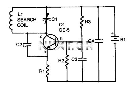
The locator utilizes a transistor radio as the detector. By tuning the radio to a weak station, the capacitor C1 can be adjusted so that the locator's oscillator beats against the received signal. When the search head passes over...
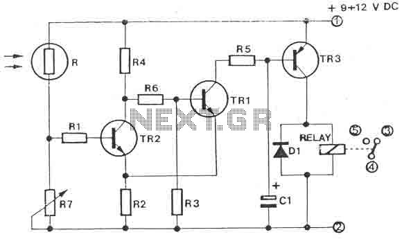
The circuit is a light switch that activates when the light intensity drops on a photoresistor. It features a straightforward construction and can be utilized in numerous applications. The photoresistor and the trimmer function as a voltage divider and...
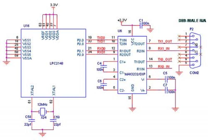
The interfacing of a Bluetooth module with the LPC2148 microcontroller is a straightforward process that enables the transmission of messages from the LPC2148 Primer Board to mobile devices via Bluetooth using UART0. Some delays may occur when sending a...
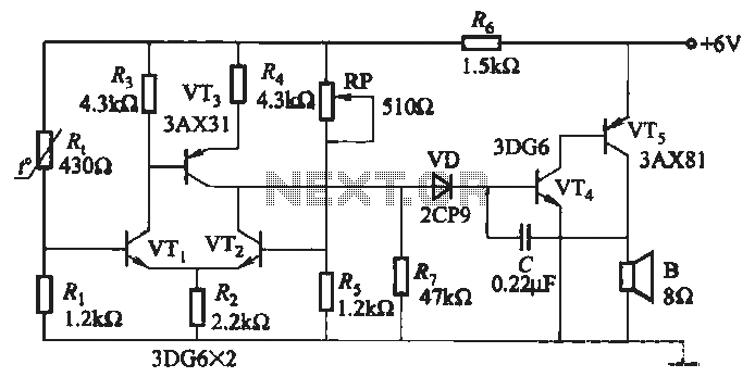
A negative temperature coefficient thermistor is utilized as the temperature sensing element (Rt). The circuit includes a resistor (Ri), a resistor (Rs), a potentiometer (RP), and the thermistor (R) to form a temperature bridge. A differential amplifier is created...
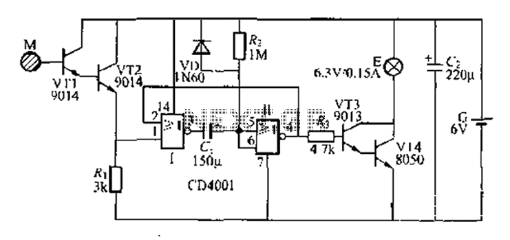
A two-battery powered light touch delay circuit designed for convenience at night. It can be placed on a bed pillow, and when the metal contact M under the capsule is touched, a small lamp will automatically light up. The...
Have you ever observed the stairs to an upper story in your house transform into a waterfall? Or perhaps you returned home to find your aquarium fish attempting to swim across the carpet? For your sake, it is hoped...