
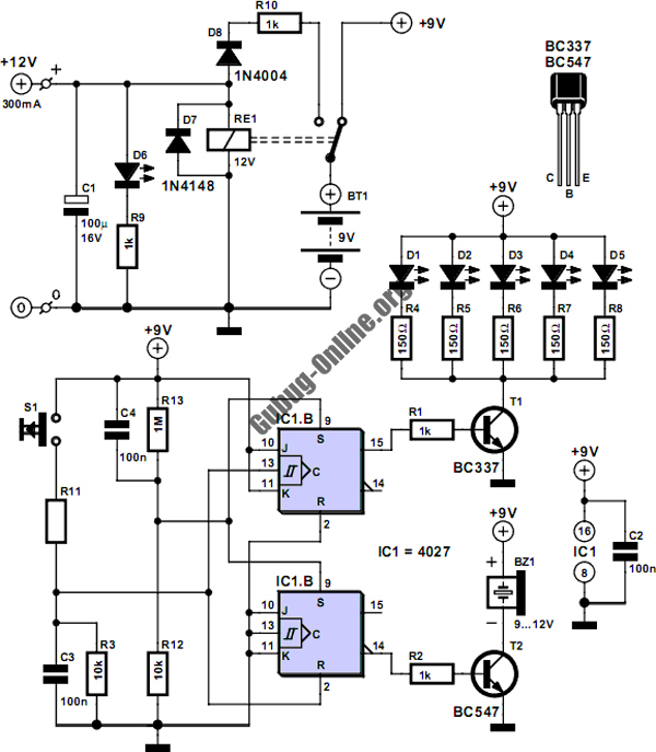
Safety Circuit Circuit
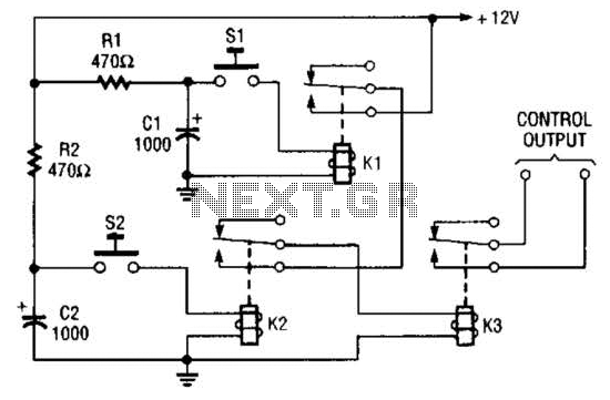
The circuit in question involves a delay mechanism governed by the time constants associated with the resistors and capacitors, specifically R1/C1 and R2/C2. The finite hold-on time implies that once the switches S1 and S2 are pressed, the circuit will only maintain the power to the load for a limited duration, dictated by the RC time constants.
In practical terms, R1 and C1 form a delay circuit that controls the first part of the system, while R2 and C2 manage the second part. The simultaneous activation of S1 and S2 ensures that both delay circuits are engaged, allowing the load to receive power effectively. If either switch is activated independently, the load will not receive the necessary power, potentially leading to system failure or undesired behavior.
To design this circuit effectively, it is essential to calculate the appropriate values for the resistors and capacitors to achieve the desired hold-on time. The time constant (τ) for each RC circuit is calculated using the formula τ = R × C, where R is the resistance in ohms and C is the capacitance in farads. By selecting suitable values for R1, C1, R2, and C2, the circuit can be tailored to meet specific operational requirements.
Additionally, considerations should be made regarding the switch ratings, as S1 and S2 must be capable of handling the load current without failure. The overall design should also include protection mechanisms, such as diodes for flyback protection if inductive loads are involved, to safeguard the circuit against voltage spikes that could occur during switching.
In summary, this circuit's functionality hinges on the precise coordination of the delay circuits and the simultaneous activation of the switches, ensuring reliable power delivery to the load within the specified time constraints. Because of the finite hold-on time of delay circuits Rl/Cl and R2/C2, both SI and S2 must be pressed at the same time to power up the load. 🔗 External reference
Related Circuits
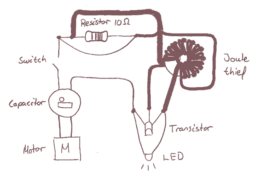
Early in the electronics design process, the decision was made to implement a joule saver in the circuit. The intention of using a joule saver is to maintain the LED light illumination even after the handle is no longer...
By adjusting the oscillators so their frequencies are very nearly the same, the difference between them is made audible as a beat note. This beat note changes slightly when the search loop is moved over or near to a...
In audio systems, noise signals are generally undesirable, and efforts are often made to eliminate them. Transistors can be utilized effectively for this purpose due to their availability and low noise characteristics. The following circuit serves as a Noise...
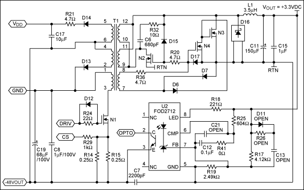
A PoE Plus power level of 30 W can be achieved by utilizing an external MOSFET along with a controller that is compatible with the older standard. Power over Ethernet (PoE) technology enables the delivery of electrical power along with...
This circuit is designed to control the mains pulse. The pulser's purpose is to switch the mains voltage on and off at intervals ranging from just under one second to a maximum of ten minutes. This functionality is beneficial...
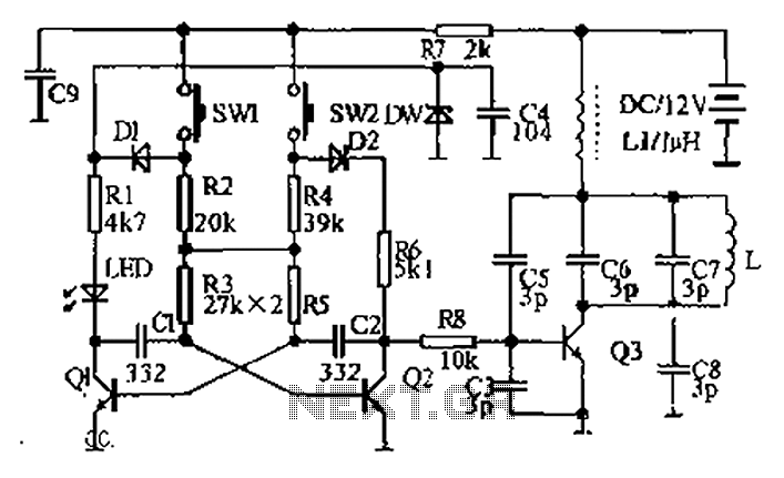
The circuit diagram illustrates a dual radio remote control switch system. The transmitter section features Q3, which generates a high-frequency carrier signal, while Q1 and Q2 form the oscillator circuit. Pressing switch SW1 results in an oscillation frequency of...
Warning: include(partials/cookie-banner.php): Failed to open stream: Permission denied in /var/www/html/nextgr/view-circuit.php on line 713
Warning: include(): Failed opening 'partials/cookie-banner.php' for inclusion (include_path='.:/usr/share/php') in /var/www/html/nextgr/view-circuit.php on line 713