
Simple 100W InverterCircuit Based On The CD4047 IC
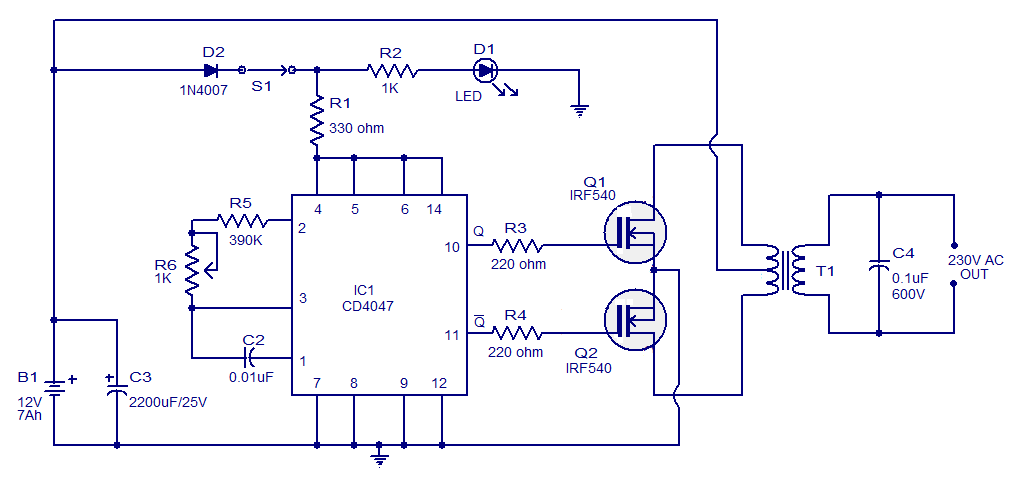
The simple 100W inverter circuit utilizes the CD4047 IC, which is a versatile device capable of generating square wave signals. This circuit is primarily designed to convert a DC input voltage into an AC output voltage, making it suitable for various applications such as powering small appliances or providing backup power.
The CD4047 can operate in either astable or monostable mode, with the astable mode being used in this application to create a continuous square wave output. The frequency of the output waveform can be adjusted by changing the values of the external resistors and capacitors connected to the IC. This flexibility allows for customization based on the specific requirements of the load.
The circuit typically includes additional components such as transistors, which are used to amplify the output signal from the CD4047 and drive the transformer. The transformer steps up the voltage to the desired level, delivering an AC output suitable for the intended application.
The inverter circuit may also incorporate protection features, such as fuses or circuit breakers, to prevent damage from overload conditions. Furthermore, the use of low power CMOS technology ensures that the circuit operates efficiently, minimizing power loss and heat generation.
Overall, this 100W inverter circuit is an effective solution for converting DC power to AC power, leveraging the capabilities of the CD4047 IC for reliable performance in various electronic applications.The following circuit Shows about Simple 100W Inverter Circuit Diagram. This circuit based on the CD4047 IC. Features: low power CMOS .. 🔗 External reference
Related Circuits

The operation principle of the proposed metal detector circuit is straightforward yet intriguing. The detection function is activated by sensing a decrease in the quality factor (Q) of the LC network associated with the circuit when a metal object...
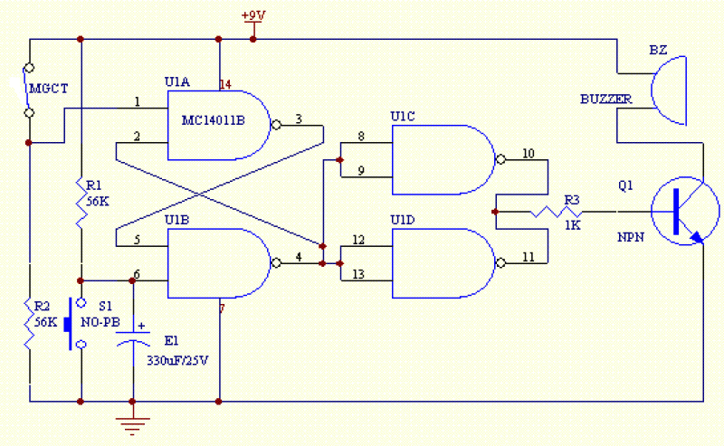
The circuit shown below is a basic latching circuit consisting of a quad 2-input NAND Gate IC. It is configured such that the flip flop circuit U1A and U1B has both its input held at logic "1". Pin 1...
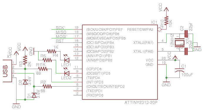
This is a low-cost AVR programmer using the ATtiny2313. The schematic diagram is provided below. First, set up the circuit as shown. One important consideration is to configure the fuse bits using the command: avrdude -c usbasp -p t2313...
The loads consist of two or more solenoids connected in parallel, sharing a 12V supply. Each solenoid is individually switched to ground through the vehicle's ECU. The objective is to detect when any one of the circuits closes, ensuring...
This weblog discusses electronic circuit schematics, PCB design, DIY kits, and electronic project diagrams. The subject circuit is a quality preamplifier with a built-in USB DAC designed for the Leachamp power amplifier. The schematic is based on the PCM2902...
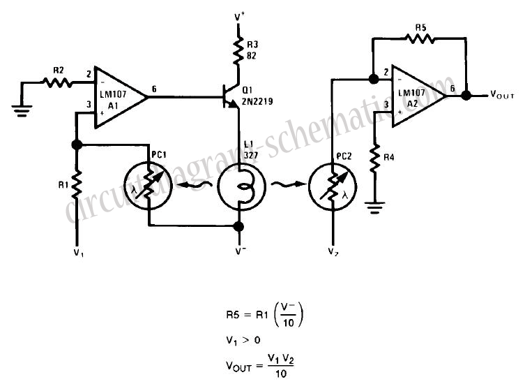
This circuit is a simple analog multiplier. The operation of the circuit can be understood by considering A2 as a controlled gain amplifier that amplifies V2, with its gain dependent on the ratio of the resistance of PC2 to...