
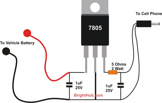
Simple Transistor Amplifier Circuit Schematic and Explanation
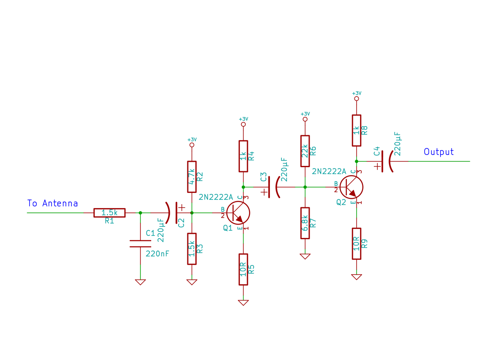
The circuit operates as a basic common-emitter amplifier, which is a fundamental configuration in analog electronics. In this setup, the input signal is applied to the base of the transistor, while the amplified output signal is taken from the collector. The low-pass filter formed by R1 and C1 is crucial for filtering out high-frequency noise, which can adversely affect the performance of the amplifier by introducing unwanted signals. The cutoff frequency of the filter can be calculated using the formula:
\[ f_c = \frac{1}{2\pi RC} \]
where \( R \) is the resistance in ohms and \( C \) is the capacitance in farads. This relationship allows for the design of the circuit to be tailored to specific applications by selecting appropriate resistor and capacitor values.
The biasing of the transistors is essential for ensuring that they operate in the active region, where they can provide linear amplification. The biasing network formed by R2 and R3 for Q1 and the corresponding resistors for Q2 ensures that the transistors are correctly biased, enhancing performance and stability. The gain of the amplifier can be adjusted by varying the values of the collector and emitter resistors, allowing for flexibility in amplification depending on the application needs.
It is also important to consider the power supply voltage when designing the circuit, as it affects the maximum output signal swing. The overall design should ensure that the transistors do not saturate or enter cutoff during operation, which would result in distortion of the amplified signal. Proper thermal management should also be considered, especially if the circuit is intended for prolonged use or high signal levels, to prevent overheating and ensure reliability.
In summary, this transistor amplifier circuit provides a foundation for understanding signal amplification in electronics, with opportunities for further optimization and enhancement based on specific application requirements.This circuit doesn`t work as well as it could. I made it when I had a lesser understanding of circuit design. I`ll probably make a new and improved schematic and post later on, one that has a better design. Thanks for stopping by! Note: The schematic here says antenna , but that`s because it was used specifically to amplify electrical noise in t he environment. The circuit is explained below, and it`s easy to use as a simple signal amplifier for anything. One thing I`ve noticed about electronics is the lack of simple, newbie-friendly information on the internet about specific topics. Then again, maybe I just wasn`t looking properly. To help fill this possibly existent information gap, I`m going to post a nice, simple schematic and an explanation on what it is and how it works.
This post goes along with a video that I posted. You don`t need to watch the video to understand the circuit, but the videodemonstratesthe circuit in action. Here it is: Okay, first thing: Right click on the image and open it in a new tab or window; it will make it easier to see it and compare it to what I`m writing.
I will explain the function of each part of the circuit. For those who are interested, the schematic was done with the free electronics design suite, Kicad. The circuit you see here is a transistor amplifier circuit. It`s identical to the one seen in the video. This very simple circuit can be used to amplify signals of all kinds. Audio, radio, whatever. You may notice that it says To antenna . This is because in the video, it was used to amplify electrical noise. The 1. 5k resistor R1 and the 220nF capacitor C1 form a low-pass filter. A low pass filter, in brief, is a filter that only allows signals lower than the cut-off frequency to pass through. I used this because without the filter, it would pick up AM radio signals and distort the noise (hehe).
If you remove that, then you`ll hear a bunch of jumbled AM radio signals. It`s pretty cool! The low-pass filter`s cutoff frequency is determined by a formula that involves the value of the resistor and capacitor used. It`s called an RC Filter (Because of the Resistor and the Capacitor). You can find many calculators online for the cutoff frequency of such a filter, just look up RC filter calculator .
Unless you want to attenuate all frequencies above ~500Hz, you should remove or change these components for optimal performance. The capacitor C2 is there to block DC from the circuit. The value of 220uF is good for passing audio frequencies with minimal impedance (Higher value = lower frequencies, take a look at capacitive reactance).
The two resistors R2 and R3 are a voltage divider, this is needed to bias the transistor. Biasing a transistor means to give the transistor enough voltage that it`s partly on, but not so much that it turns on fully. This is necessary for an amplifier. Q1 is a 2N2222A NPN transistor. The collector resistor (The collector is the one without the arrow) and the emitter resistor set the gain of the transistor.
The gain can be approximated with -Rc/Re (The minus is there because the signal is inverted with this amplifier). Rc is the collector resistor, and Re is the emitter resistor. In this case, the gain is ~100 (~ means approximately). Q2 is the same as Q1, and the resistors around it have the same function. The voltage divider uses different value resistors, but that`s only because I didn`t have enough resistors of the same type as the voltage divider on Q1 (They were in use on some other projects).
The Q2 voltage divider gives roughly the same voltage output as the Q1 divider. There are two transistors because each one amplifies the signal more. You might think Why can`t I just use one transistor with a really big collector resistor . That`s an excellent question. You can`t make the collector resistor (Rc) too big, because in a common-emitteramplifier (Which is what this circuit uses), Rc sets the outpu 🔗 External reference
Related Circuits
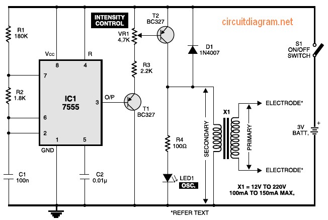
Figure 1 shows the circuit of a muscular stimulator. The IC 7555 is configured as an astable multivibrator to generate approximately 80Hz pulses. The output from IC1 is connected to transistor T1, whose emitter is linked to the base...
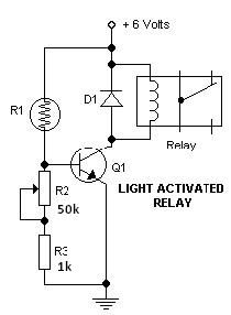
This light-dark switch activated relay circuit schematic represents one of the simplest electronic circuits designed to activate other electronic devices based on light or darkness. It requires a single electronic relay and a few common components that are not...
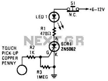
When the touch-on contacts are bridged, pin 6 of U1 goes low, which forces its output (the set output) at pin 4 to go high. That high divides along two paths; in one path, the output is applied to...
With the advent of modern integrated circuits (ICs), sophisticated circuits today are no longer required to be complex and lengthy. The chips themselves contain most of the intricate circuitry built-in and can independently perform the desired functions. For instance,...
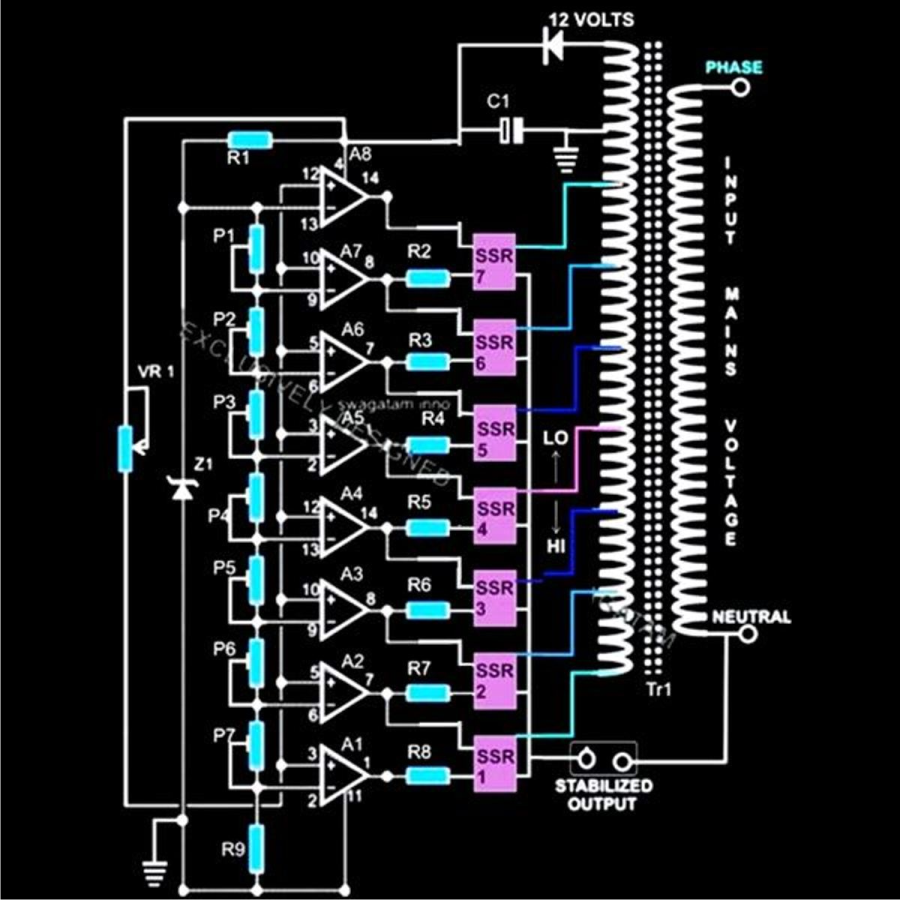
The diagram illustrates a straightforward voltage stabilizer design capable of handling significant output power in the range of 5 to 10 KVA. The implementation of solid-state relays (SSRs) simplifies the output stage configuration and enhances accuracy, owing to modern...
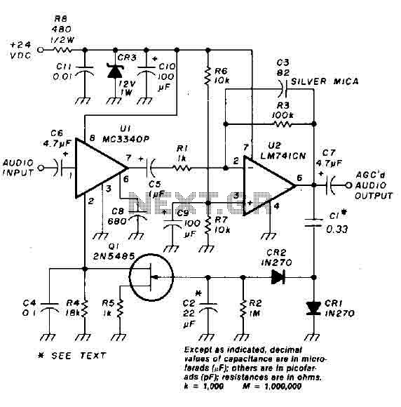
An audio signal applied to the input VI is passed through the operational amplifier 741, designated as U2. After amplification, the output signal V2 is sampled and sent to a negative voltage doubler/rectifier circuit composed of diodes CR1 and...
Warning: include(partials/cookie-banner.php): Failed to open stream: Permission denied in /var/www/html/nextgr/view-circuit.php on line 713
Warning: include(): Failed opening 'partials/cookie-banner.php' for inclusion (include_path='.:/usr/share/php') in /var/www/html/nextgr/view-circuit.php on line 713