
Transistor Tutorial MOSFETs

The MOSFET operates by controlling the conductivity of a channel between the source and drain terminals through an electric field generated by the gate voltage. In the enhancement-mode configuration, a positive gate voltage attracts electrons to the channel region in an N-channel device, thereby allowing current to flow when the device is activated. Conversely, in a P-channel MOSFET, a negative gate voltage is required to create a conductive channel by attracting holes.
The switching speed of MOSFETs is a critical aspect in applications such as digital circuits and power management systems. The lower on-resistance of N-channel MOSFETs compared to P-channel MOSFETs contributes to their preference in high-speed applications. Additionally, the complementary nature of N- and P-channel MOSFETs allows for efficient push-pull configurations in CMOS technology, minimizing power consumption and enhancing performance in integrated circuits.
In practical applications, the selection between N-channel and P-channel MOSFETs typically depends on the specific requirements of the circuit, including voltage levels, switching speed, and power handling capabilities. Circuit designers often utilize enhancement-mode MOSFETs in various configurations, such as common-source, common-drain, or common-gate amplifiers, to achieve desired amplification characteristics and signal processing capabilities. The versatility of MOSFETs makes them indispensable in modern electronic design, providing reliable performance across a wide range of applications.The Metal-Oxide-Semiconductor Field-Effect Transistor, or MOSFET for short, is similar in many ways to the junction FET (JFET). Both are voltage-driven unipolar devices that depend on either electron or hole movement-but not both, as does the bipolar transistor.
However, there is a fundamental structural difference between the two field-effect tr ansistors: The JFET has three layers while the MOSFET has two. The MOSFET`s simpler construction has give it a performance edge over the JFET, and made it the world`s most popular transistor style. Earlier articles in this series stated that the MOSFET`s controlling gate voltage is applied directly to its channel region across a thin layer of insulating oxide, as shown in Fig.
1-a. This geometry contrasts with that of the JFET, which is controlled by switching an internal PN junction. The MOSFET will work from lower power that the JFET, and its simpler design is reflected in lower production costs.
That is why it has become the basis for all CMOS digital logic IC families. Part 9 and Part 11 in this series discussed FET`s. The basic principles of JFET`s and MOSFET`s were explained in the first article of (Electronics Now, February 1993) and the words that describe them were defined. The second article (Electronics Now, March 1993) focused on JFET`s, and included practical JFET circuit schematics.
This article concentrates on the enhancement-mode MOSFET, and it includes practical MOSFET circuit schematics base upon small-signal MOS transistors available in a low-cost CMOS integrated circuit. You might wish to review the first two articles to refresh your general knowledge of FET`s before reading this article.
There are both N- and P-channel MOSFET`s just as there are both N- and P-channel JFET`s. In the cross-section view of an N-type enhancement-mode transistor, Fig. 1a, you can see the thin layer of silicon dioxide (glass) that electrically isolates the metal gate from the channel between the N-doped source and drain regions. The presence of that insulated gate is why the MOSFET has also been called and IGFET (for insulated gate FET).
However, that term is now considered obsolete. As shown in Fig. 1a, the channel between the N-type source and drain of an N-channel, enhancement-mode MOSFET is the substrate P-type material. This MOSFET can be turned on so that current flows between source and drain only when a positive forward bias is placed on the gate.
As a result, the enhancement-mode MOSFET is said to be "normally off". Its operation depends on the electron flow. Recall, from Part 9`s article, that all JFET`s are depletion-mode or "normally on" devices. They are turned `off` by applying reverse bias. Depletion-mode MOSFET`s are being made today for high-frequency radio applications. A P-channel, enhancement-mode MOSFET has a cross section that is identical to that shown in Fig. 1-a except that the substrate is N-type material and the source and drain regions are P-type material. A negative forward bias is needed to turn a P-channel, enhancement-mode MOSFET ON. Its operation depends on the movement of holes, which have lower mobility than electrons. This means that an N-channel MOSFET can switch faster than a P-channel MOSFET. As in the JFET, signal voltages or biases applied between the gate and source terminals of the MOSFET control the magnitudes of signal currents flowing between the drain and source terminals.
N- and P-channel MOSFET`s are said to be complementary because the doping of their substrate, source, and drain materials as well as their forward bias polarities are opposite. Figure 1-b is the schematic symbol for an enhancement-mode N-channel MOSFET. The dotted vertical line between the drain and the source represents a "normally-off" channel. (The symbol for complementary P-channel device is similar except that its arrow points outwards. ) Figure 2-a shows a cross section of a monolithic CMOS IC with both 🔗 External reference
Related Circuits
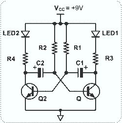
This circuit is straightforward and easy to construct, utilizing two transistors as active components along with several passive components such as resistors, capacitors, and two LEDs. The circuit employs the MPS2222 transistor, though any NPN type transistor can be...
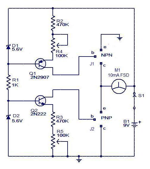
The circuit for a transistor tester is a relatively simple device. The transistor tester circuit illustrated below can be utilized to measure and identify the pins of a transistor, as well as determine its condition. Furthermore, this circuit can...
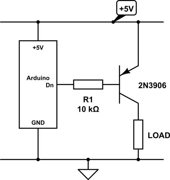
The emitter will consistently be a few hundred millivolts lower than the base voltage in this configuration. With the base voltage set at 5V, the emitter voltage is likely to be around 4.5V, depending on the current drawn by...
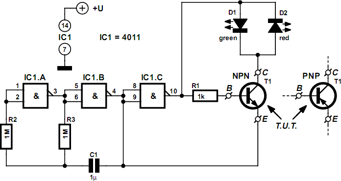
This small transistor tester employs a simple visual indication system to perform a quick go/no-go check on both NPN and PNP transistors. When testing a functioning NPN transistor, the green LED (D1) will flash, while the red LED will...
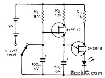
The following circuit illustrates a flashing LED egg timer circuit diagram. This circuit utilizes 2N2646 transistors and features an MPF112 FET. The flashing LED egg timer circuit operates as a visual timer, providing an indication of elapsed time through the...
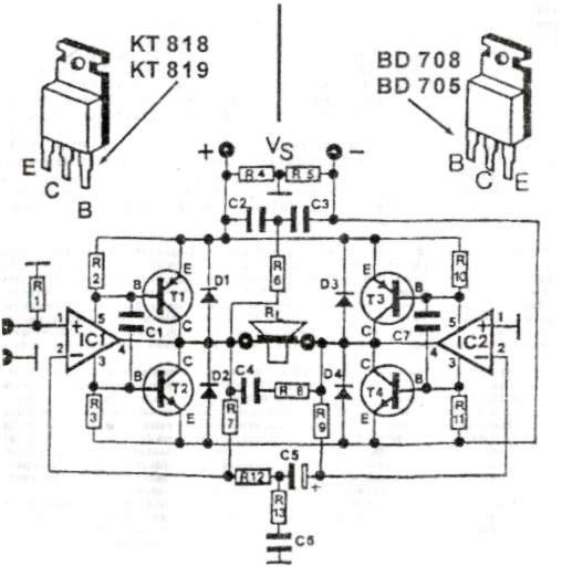
This audio amplifier circuit provides up to 200 W of high-quality output for loudspeakers with impedances ranging from 4 to 16 ohms. The operating voltage is between 24 and 36 V, with a maximum current of 5 A. The audio...