
variable 4 a25v power supply

The circuit design is structured in three distinct stages, each serving a specific function essential for the overall operation of the power supply. The first stage initiates the process by utilizing a transformer to step down the input voltage to a safer level. This is followed by a bridge rectifier, which converts the alternating current (AC) output from the transformer into direct current (DC). The 10,000 µF electrolytic capacitor plays a critical role in smoothing the rectified voltage, effectively filtering out ripples and providing a stable DC output suitable for subsequent stages.
In the second stage, the circuit employs BC327 transistors, which are bipolar junction transistors (BJTs) known for their efficiency in switching and amplification applications. These transistors are integrated with additional components to form a reference voltage generator. The reference voltage is crucial as it sets the operating conditions for the driver transistor. The inclusion of a potentiometer allows for adjustable voltage levels, providing flexibility in the output power. The configuration of a top resistor in conjunction with the potentiometer ensures precise control over the voltage applied to the driver transistor, thereby regulating the power output.
The design features a resistive and non-switched control mechanism, which results in a pulsed voltage at the emitter of the driver transistor. This pulsed output is vital for applications requiring variable power levels. To ensure the integrity of the output signal, a small output filter, consisting of an electrolytic capacitor, is incorporated at the output terminals. This filter mitigates any high-frequency noise, ensuring a clean and stable output voltage.
In summary, this circuit design effectively combines isolation, voltage regulation, and filtering to produce a reliable variable power supply capable of delivering up to 4 A at 25 V. The schematic serves as a valuable reference for understanding the intricate workings of the power supply and the roles played by each component within the circuit. Further insights and details can be explored on the dedicated webpage, enhancing comprehension of the circuit's functionality and applications.As shown in the scheme that the circuit consists of three stages. The first (which is formed by a transformer, bridge rectifier and an electrolytic capacitor 10000 F) is responsible for isolating and reduce the voltage, improve and filter. The second phase (consisting of, BC327 transistor integrated circuits and components attached) is responsibl
e for providing a reference voltage which is used to determine, together with the potentiometer and top resistor, voltage applied to the driver transistor and power. It should be noted that they made a resistive and non-switched control (switching) so the voltage at the emitter is pulsed.
Then we have a small output filter formed by the electrolytic capacitor and terminals. The schematic diagram come from circuit: Variable 4 A/25V Power Supply power supply. Go to that page to read the explanation about above power supply related circuit diagram. 🔗 External reference
Related Circuits
The 2SK2975 has reportedly been discontinued by the manufacturer, with the RD07MVS1 from Mitsubishi serving as its replacement. This new device is very similar but appears to have slightly higher gain—10 dB typical at 520 MHz compared to 8.4...
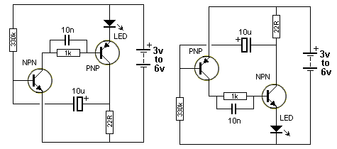
The circuit involves powering an LED using a 3V CR2032 battery, with the intention of extending battery life by making the LED blink rather than remain continuously on. A 555 timer is considered, utilizing large value resistors in the...

A repertory dialer phone contains a library of phone numbers that can be entered and dialed, allowing access to up to fifteen frequently used numbers. It also includes the capability to store the last dialed number or an additional...
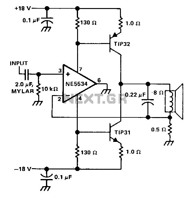
The single speaker amplifier circuit utilizes current feedback instead of the more commonly used voltage feedback. The feedback loop originates from the junction of the speaker terminal and a 0.5-ohm resistor, connecting to the inverting input of the NE5534...
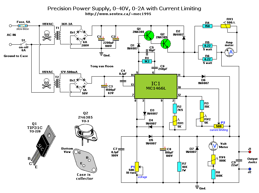
This precision power supply is a valuable addition to any workbench, serving as either a primary or supplementary power supply. It offers a voltage range of 0 to 40V and a current capacity of 2A, with adjustable current limiting...
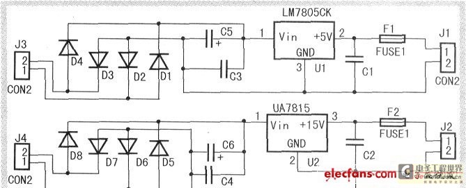
When the input voltage is between 198-242V, the average load current should be maintained at 0.5-1A, and the output voltage must remain at 15V with an error margin of less than 5%. The design and measurement of the stabilized...
Warning: include(partials/cookie-banner.php): Failed to open stream: Permission denied in /var/www/html/nextgr/view-circuit.php on line 713
Warning: include(): Failed opening 'partials/cookie-banner.php' for inclusion (include_path='.:/usr/share/php') in /var/www/html/nextgr/view-circuit.php on line 713