
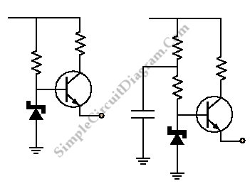
voltage transistor loop to limit the current

The circuit utilizes two transistors, T1 and T2, to regulate the current flowing through a load, ensuring that it does not exceed a predefined limit of 250 mA. Transistor T1 acts as the primary power switch, while T2 serves as a control switch that responds to the voltage developed across resistor R1.
Resistor R1 is strategically placed in series with the load and is responsible for sensing the current. The relationship between the current flowing through R1 and the voltage across it is defined by Ohm's law (V = I × R). With R1 set to 2.7 ohms, the voltage drop across the resistor when the current reaches 250 mA can be calculated as follows:
V = I × R = 0.250 A × 2.7 Ω = 0.675 V.
This voltage drop is sufficient to turn on transistor T2, which is configured in a way that its base is connected to the junction of R1 and the load. When T2 is activated, it effectively pulls the base of T1 low, turning T1 off and thus limiting the current to the load.
The DALI (Digital Addressable Lighting Interface) slave unit's connection ensures that the current through R1 reflects the operational state of the entire circuit. As the current approaches the threshold of 250 mA, the design guarantees that T2 will activate, thereby protecting the circuit from excessive current that could lead to damage or failure.
The logic levels of 12V for high and 0V for low in this design indicate the operational states of the control signals, allowing for digital communication within the circuit. This setup is essential for applications in lighting control systems where precise current regulation is necessary to maintain the integrity and functionality of the connected devices.The other transistor (T2) is controlled by the current flowing through the resistor (R1). If a DALI slave unit is connected, this current will be the same as that flowing through the power transistor. The value of the resistor is chosen in such a way that when the current exceeds 250 mA the voltage level across the resistor will open the transisto
r (T2) which in its turn closes the power transistor (T1). In this way the current is maximized to 250 mA. Could anyone explain me how does the resistor R1 (in the first picture) value 2. 7 ohm opens the transistor when the current exceeds 250mA On that design, the signal is transmitted as 12V (logic high) and 0V (logic low). 🔗 External reference
Related Circuits

This tester checks the polarity of transistors (PNP or NPN). An audible signal indicates the gain. Additionally, the tester can function as a GO/NO GO tester for matching unmarked devices. The transistor tester is designed to evaluate the polarity and...
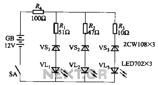
When the supply voltage falls below 10.2V, the yellow light-emitting diode (LED) VLi illuminates, indicating that the storage pool can no longer continue to discharge. Additionally, when the voltage exceeds 16.2V, the yellow, green, and red light-emitting diodes (LEDs)...
The circuit diagram represents a brushless DC motor driving circuit designed for a 45V/8A application. It features an open voltage-controlled design that allows for speed adjustment through an external potentiometer connected to a PWM duty cycle. The diagram illustrates...
This circuit detects when a tube is empty and pulses a piezo buzzer at 5-second intervals. It is currently operational with a 5V supply on a breadboard but needs to be adapted for a 12V supply from a wall...
Buffering for the zener diode is achieved through the impedance matching and current amplifying features of the emitter follower, which draws less current from the zener. Buffering in electronic circuits is essential for ensuring that the performance of one component...
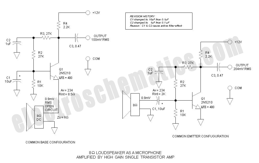
Single Transistor Amplifier Revisited Part 3, Common Base vs Common Emitter Configuration, Update One nagging question that I have long had is this: How do... The single transistor amplifier is a fundamental building block in electronic circuits, and its configurations—common...